Characteristics of N-Channel JFET | Analog and Digital Electronics - Electrical Engineering (EE) PDF Download

CHARACTERISTICS OF N-CHANNEL JFET :-
The family of curves that shows the relation between current and voltage are known as characteristic curves.
There are two important characteristics of a JFET.
- Drain or VI Characteristics
- Transfer characteristics
Drain Characteristics:-
Drain characteristics show the relation between the drain to source voltage Vds and drain current Id. In order to explain typical drain characteristics let us consider the curve with Vgs= 0 V.
1. When Vds is applied and it is increasing the drain current Id also increases linearly up to knee point.
2. This shows that FET behaves like an ordinary resistor. This region is called as ohmic region.
3. Id increases with increase in drain to source voltage. Here the drain current is increased slowly as compared to ohmic region.
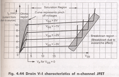
4. It is because of the fact that there is an increase in Vds. This in turn increases the reverse bias voltage across the gate source junction. As a result of this depletion region grows in size thereby reducing the effective width of the channel.
5. All the drain to source voltage corresponding to point the channel width is reduced to a minimum value and is known as pinch off.
6. The drain to source voltage at which channel pinch off occurs is called pinch off voltage(Vp).
PINCH OFF Region:-
- This is the region shown by the curve as saturation region.
- It is also called as saturation region or constant current region. Because of the channel is occupied with depletion region , the depletion region is more towards the drain and less towards the source, so the channel is limited, with this only limited number of carriers are only allowed to cross this channel from source drain causing a current that is constant in this region. To use FET as an amplifier it is operated in this saturation region.
- In this drain current remains constant at its maximum value Idss.
- The drain current in the pinch off region depends upon the gate to source voltage and is given by the relation-
Id =Idss [1-Vgs/Vp]2
This is known as shokley’s relation.
BREAKDOWN REGION:-
- The region is shown by the curve. In this region, the drain current increases rapidly as the drain to source voltage is increased.
- It is because of the gate to source junction due to avalanche effect.
- The avalanche break down occurs at progressively lower value of Vds because the reverse bias gate voltage adds to the drain voltage thereby increasing effective voltage across the gate junction. This causes
- The maximum saturation drain current is smaller.
- The ohmic region portion decreased.
- It is important to note that the maximum voltage Vds which can be applied to FET is the lowest voltage which causes available breakdown.
TRANSFER CHARACTERISTICS:-
These curves show the relationship between drain current Id and gate to source voltage Vgs for different values of Vds.
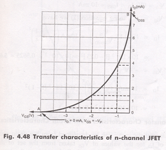
- First adjust the drain to source voltage to some suitable value , then increase the gate to source voltage in small suitable value.
- Plot the graph between gate to source voltage along the horizontal axis and current Id on the vertical axis. We shall obtain a curve like this.
- As we know that if Vgs is more negative curves drain current to reduce . where Vgs is made sufficiently negative, Id is reduced to zero. This is caused by the widening of the depletion region to a point where it is completely closes the channel. The value of Vgs at the cutoff point is designed as Vgsoff
- The upper end of the curve as shown by the drain current value is equal to Idss that is when Vgs = 0 the drain current is maximum.
- While the lower end is indicated by a voltage equal to Vgsoff
- If Vgs continuously increasing , the channel width is reduced , then Id =0
- It may be noted that curve is part of the parabola; it may be expressed as-
Id=Idss[1-Vgs/Vgsoff]2
DIFFERENCE BETWEEN Vp AND Vgsoff –
Vp is the value of Vgs that causes the JFET to become constant current component, It is measured at Vgs=0 V and has a constant drain current of Id =Idss .Where Vgsoff is the value of Vgs that reduces Id to approximately zero.
Why the gate to source junction of a JFET be always reverse biased ?
The gate to source junction of a JFET is never allowed to become forward biased because the gate material is not designed to handle any significant amount of current. If the junction is allowed to become forward biased, current is generated through the gate material. This current may destroy the component.
There is one more important characteristic of JFET reverse biasing i.e. JFET's have extremely high characteristic gate input impedance. This impedance is typically in the high mega ohm range. With the advantage of extremely high input impedance it draws no current from the source. The high input impedance of the JFET has led to its extensive use in integrated circuits. The low current requirements of the component makes it perfect for use in ICs where thousands of transistors must be etched on to a single piece of silicon. The low value of current helps the IC to remain relatively cool, thus allowing more components to be placed in a smaller physical area.
JFET PARAMETERS
The electrical behavior of JFET may be described in terms of certain parameters. Such parameters are obtained from the characteristic curves.
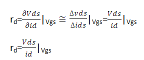
A C Drain resistance(rd):
It is also called dynamic drain resistance and is the a.c.resistance between the drain and source terminal,when the JFET is operating in the pinch off or saturation region. It is given by the ratio of small change in drain to source voltage ∆Vds to the corresponding change in drain current ∆Id for a constant gate to source voltage Vgs.
Mathematically, it is expressed as rd=∆Vds/ ∆Id where Vgs is held constant.
TRANSCONDUCTANCE (gm):
It is also called forward transconductance. It is given by the ratio of small change in drain current (∆Id) to the corresponding change in gate to source voltage (∆Vds)
Mathematically, the transconductance can be written as-
gm=∆Id/∆Vds
AMPLIFICATION FACTOR (µ)
It is given by the ratio of small change in drain to source voltage (∆Vds) to the corresponding change in gate to source voltage (∆Vgs)for a constant drain current (Id).
Thus µ=∆Vds/∆Vgs when Id held constant
The amplification factor µ may be expressed as a product of transconductance (gm)and ac drain resistance (rd)-
µ=∆Vds/∆Vgs=gm rd
THE FET SMALL SIGNAL MODEL:-
The linear small signal equivalent circuit for the FET can be obtained in a manner similar to that used to derive the corresponding model for a transistor.
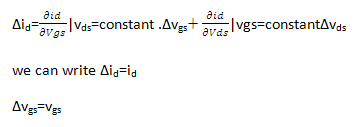
We can express the drain current Id as a function of the gate voltage and drain voltage Vds.
Id =f(Vgs,Vds)------------------(1)
The transconductance gm and drain resistance rd:-
If both gate voltage and drain voltage are varied, the change in the drain current is approximated by using Taylor's series considering only the first two terms in the expansion:
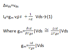
Is the mutual conductance or transconductance .It is also called as gfs or yfs common source forward conductance .
The second parameter rd is the drain resistance or output resistance defined as:
The reciprocal of the rd is the drain conductance gd. It is also designated by Yos and Gos and called the common source output conductance . So the small signal equivalent circuit for FET can be drawn in two different ways:
1.small signal current –source model
2.small signal voltage-source model.
A small signal current –source model for FET in common source configuration can be drawn satisfying Eq→(1) as shown in the figure(a)
This low frequency model for FET has a Norton’s output circuit with a dependent current generator whose magnitude is proportional to the gate-to-source voltage. The proportionality factor is the transconductance ‘gm’. The output resistance is ‘rd’. The input resistance between the gate and source is infinite, since it is assumed that the reverse biased gate draws no current. For the same reason the resistance between gate and drain is assumed to be infinite.
The small signal voltage-source model is shown in the figure(b).
This can be derived by finding the Thevenin’s equivalent for the output part of fig(a) .
These small signal models for FET can be used for analyzing the three basic FET amplifier configurations:
1.common source (CS) 2.common drain (CD) or source follower
3. common gate(CG).
(a)Small Signal Current source model for FET (b)Small Signal voltage source model for FET
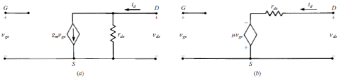
Here the input circuit is kept open because of having high input impedance and the output circuit satisfies the equation for Id.
|
135 videos|181 docs|71 tests
|
FAQs on Characteristics of N-Channel JFET - Analog and Digital Electronics - Electrical Engineering (EE)
| 1. What is an N-Channel JFET? |  |
| 2. How does an N-Channel JFET work? | |
| 3. What are the advantages of using an N-Channel JFET? | |
| 4. What are the limitations of N-Channel JFETs? | |
| 5. What are some common applications of N-Channel JFETs? | |


Characteristics of N-Channel JFET | Analog and Digital Electronics - Electrical Engineering (EE)
,practice quizzes
,mock tests for examination
,Sample Paper
,Characteristics of N-Channel JFET | Analog and Digital Electronics - Electrical Engineering (EE)
,Characteristics of N-Channel JFET | Analog and Digital Electronics - Electrical Engineering (EE)
,Viva Questions
,MCQs
,Objective type Questions
,past year papers
,video lectures
,Exam
,ppt
,Free
,Semester Notes
,shortcuts and tricks
,Previous Year Questions with Solutions
,Summary
,study material
,Extra Questions
,Important questions
;


Characteristics of N-Channel JFET Free PDF Download
Importance of Characteristics of N-Channel JFET
Characteristics of N-Channel JFET Notes
Characteristics of N-Channel JFET Electrical Engineering (EE) Questions
Study Characteristics of N-Channel JFET on the App
|
© EduRev
|
Education Revolution
|


|


