


All Exams >
NEET >
Weekly Tests for NEET Preparation >
All Questions
All questions of February Week 3 for NEET Exam
Proteins can be classified into two types on the basis of their molecular shape i.e., fibrous proteins and globular proteins. Examples of globular proteins are :
(Multiple Answer Correct)
- a)Insulin & Albumin
- b)Myosin
- c)Keratin
- d)None of these
Correct answer is option 'A'. Can you explain this answer?
Proteins can be classified into two types on the basis of their molecular shape i.e., fibrous proteins and globular proteins. Examples of globular proteins are :
(Multiple Answer Correct)
(Multiple Answer Correct)
a)
Insulin & Albumin
b)
Myosin
c)
Keratin
d)
None of these

|
Divey Sethi answered |
The correct answer is A and C.
The structure of protein which results when the chain of polypeptides coil around to give a spherical shape are known as globular protein. These proteins are soluble in water, e.g., insulin and albumin are globular protein.
The structure of protein which results when the chain of polypeptides coil around to give a spherical shape are known as globular protein. These proteins are soluble in water, e.g., insulin and albumin are globular protein.

Which of the following terms are correct about enzyme?
- a)Proteins
- b)Dinucleotides
- c)carbohydrates
- d)None of these
Correct answer is option 'A'. Can you explain this answer?
Which of the following terms are correct about enzyme?
a)
Proteins
b)
Dinucleotides
c)
carbohydrates
d)
None of these
|
|
Suresh Kumar answered |
Enzymes are made up of proteins...but Ribozyme is an exception to this as its made up of 23 sr RNA which is a nucleic acid...
And enzymes acts as biocatalyst...
so; more accurately option d comes out to be the answer.
And enzymes acts as biocatalyst...
so; more accurately option d comes out to be the answer.
In a semiconductor crystal, if current flows due to breakage of crystal bonds, then the semiconductor is called- a)donor
- b)acceptor
- c)extrinsic semiconductor
- d)intrinsic semiconductor
Correct answer is option 'D'. Can you explain this answer?
In a semiconductor crystal, if current flows due to breakage of crystal bonds, then the semiconductor is called
a)
donor
b)
acceptor
c)
extrinsic semiconductor
d)
intrinsic semiconductor
|
|
Preeti Iyer answered |
In the case of an intrinsic semiconductor (say Si) where each Si is having 4 outermost electrons, its crystal structure consists of making 4 covalent bonds with 4 neighbouring Si atoms. Each bond consists of two electrons.
Now if one of the bonds gets broken due to some reason (collisions or high temperature) then one electron gets free and it will be having sufficient energy to cross the band gap and be ready for conduction- So in intrinsic semiconductors, current flows due to breakage of crystal bonds.
Now if one of the bonds gets broken due to some reason (collisions or high temperature) then one electron gets free and it will be having sufficient energy to cross the band gap and be ready for conduction- So in intrinsic semiconductors, current flows due to breakage of crystal bonds.
Carbohydrates are classified on the basis of their behaviour on hydrolysis and also as reducing or non-reducing sugar. Sucrose is a __________.
- a)monosaccharide
- b)disaccharide
- c)non-reducing sugar
- d)Both b and c
Correct answer is option 'D'. Can you explain this answer?
Carbohydrates are classified on the basis of their behaviour on hydrolysis and also as reducing or non-reducing sugar. Sucrose is a __________.
a)
monosaccharide
b)
disaccharide
c)
non-reducing sugar
d)
Both b and c
|
|
Divey Sethi answered |
The correct answer is option B & D.
One of the common disaccharides is sucrose which on hydrolysis gives an equimolar mixture of D−(+)− glucose and D−(−) fructose. These two monosaccharides are held together by a glycosidic linkage between Cl of α- glucose and C2 of β- fructose. Since the reducing groups of glucose and fructose are involved in glycosidic bond formation, sucrose is a non-reducing sugar.
One of the common disaccharides is sucrose which on hydrolysis gives an equimolar mixture of D−(+)− glucose and D−(−) fructose. These two monosaccharides are held together by a glycosidic linkage between Cl of α- glucose and C2 of β- fructose. Since the reducing groups of glucose and fructose are involved in glycosidic bond formation, sucrose is a non-reducing sugar.
Three structures are given below in which two glucose units are linked. Which of these linkages between glucose units are between C1 and C4 and which linkages are between C1 and C6?
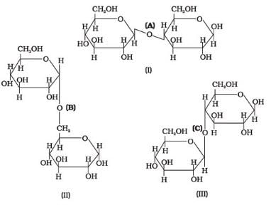
- a)(A) is between C1 and C4, (B) and (C) are between C1 and C6
- b)(A) and (B) are between C1 and C4, (C) is between C1 and C6
- c)(A) and (C) are between C1 and C4, (B) is between C1 and C6
- d)(A) and (C) are between C1 and C6, (B) is between C1 and C4
Correct answer is option 'C'. Can you explain this answer?
Three structures are given below in which two glucose units are linked. Which of these linkages between glucose units are between C1 and C4 and which linkages are between C1 and C6?
a)
(A) is between C1 and C4, (B) and (C) are between C1 and C6
b)
(A) and (B) are between C1 and C4, (C) is between C1 and C6
c)
(A) and (C) are between C1 and C4, (B) is between C1 and C6
d)
(A) and (C) are between C1 and C6, (B) is between C1 and C4
|
|
Preeti Iyer answered |
The correct answer is Option C.
(i) The first structure is lactose, the linkage is (A) C1−C4 glycosidic linkage.
(ii) The 2nd structure has C1−C6 linkages.
(iii) The 3rd structure has C1−C4 linkages.
(ii) The 2nd structure has C1−C6 linkages.
(iii) The 3rd structure has C1−C4 linkages.
In fibrous proteins, polypeptide chains are held together by ___________.
- a)van der Waals forces
- b)disulphide linkage & hydrogen bonds
- c)electrostatic forces of attraction
- d)None of these
Correct answer is option 'B'. Can you explain this answer?
In fibrous proteins, polypeptide chains are held together by ___________.
a)
van der Waals forces
b)
disulphide linkage & hydrogen bonds
c)
electrostatic forces of attraction
d)
None of these
|
|
Neha Sharma answered |
The correct answer are options B & D,
In fibrous proteins, polypeptide chains are held together by hydrogen and disulphide bonds, in parallel manner. Due to which fibre-like structure is obtained. Such proteins are generally known as fibrous proteins. These proteins are generally insoluble in water e.g., keratin, myosin.
In fibrous proteins, polypeptide chains are held together by hydrogen and disulphide bonds, in parallel manner. Due to which fibre-like structure is obtained. Such proteins are generally known as fibrous proteins. These proteins are generally insoluble in water e.g., keratin, myosin.
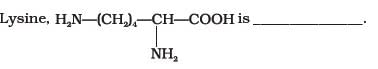
- a)α-Amino acid
- b)Basic amino acid
- c)Amino acid synthesised in body
- d)β-Amino acid
Correct answer is option 'A,B'. Can you explain this answer?
a)
α-Amino acid
b)
Basic amino acid
c)
Amino acid synthesised in body
d)
β-Amino acid

|
Sadiya Siddique answered |
In lysine,the amino group is attached to alpha carbon which makes it Alpha amino acid and it has more amino groups as compared to -COOH groups ,thus basic . so, op A,B.
The conductivity of P – type semiconductor is due to- a)both electrons and holes
- b)holes
- c)electrons
- d)none of the above.
Correct answer is option 'B'. Can you explain this answer?
The conductivity of P – type semiconductor is due to
a)
both electrons and holes
b)
holes
c)
electrons
d)
none of the above.
|
|
Lavanya Menon answered |
A P-type semiconductor is formed when a trivalent electron deficient impurities such as boron group elements are doped with intrinsic semiconductor. As the impurities are electron deficient, they take electrons from the valence band creating a number of holes. Due this reason conductivity in P-type semiconductor is mainly due to holes rather than electrons.
Which of the following are purine bases?- a)Guanine
- b)Adenine
- c)Thymine
- d)Uracil
Correct answer is option 'A,B'. Can you explain this answer?
Which of the following are purine bases?
a)
Guanine
b)
Adenine
c)
Thymine
d)
Uracil
|
|
Tanvi Bose answered |
Explanation:
Purine bases:
Purine bases are nitrogen-containing molecules that are formed by a pyrimidine ring fused to an imidazole ring. The purine bases are guanine and adenine.
Pyrimidine bases:
Pyrimidine bases consist of a single ring structure and include thymine, cytosine, and uracil.
Answer:
Therefore, the correct answer is option A and B, which are guanine and adenine. These bases are found in DNA and RNA and are important for the genetic code. Thymine is a pyrimidine base found only in DNA, while uracil is a pyrimidine base found only in RNA.
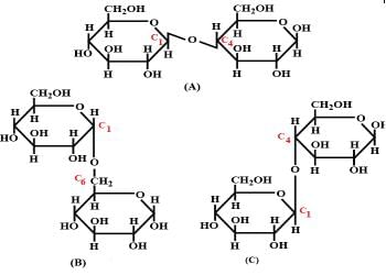
Structure of a disaccharide formed by glucose and fructose is given below. Identify anomeric carbon atoms in monosaccharide units.
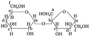
- a)‘a’ carbon of glucose and ‘a’ carbon of fructose.
- b)‘a’ carbon of glucose and ‘e’ carbon of fructose.
- c)‘a’ carbon of glucose and ‘b’ carbon of fructose.
- d)‘f ’ carbon of glucose and ‘f ’ carbon of fructose.
Correct answer is option 'C'. Can you explain this answer?
Structure of a disaccharide formed by glucose and fructose is given below. Identify anomeric carbon atoms in monosaccharide units.
a)
‘a’ carbon of glucose and ‘a’ carbon of fructose.
b)
‘a’ carbon of glucose and ‘e’ carbon of fructose.
c)
‘a’ carbon of glucose and ‘b’ carbon of fructose.
d)
‘f ’ carbon of glucose and ‘f ’ carbon of fructose.

|
Nirupama Kumari answered |
Ans - because in this case both are counted in Right Side (glucose in "a" & fructose in "b") but only single in figure fructose always counted in left side & glucose right side.
Glycogen is a branched chain polymer of α-D-glucose units in which chain is formed by C1—C4 glycosidic linkage whereas branching occurs by the formation of C1-C6 glycosidic linkage. Structure of glycogen is similar to ______.- a)Amylose
- b)Amylopectin
- c)Cellulose
- d)Glucose
Correct answer is option 'B'. Can you explain this answer?
Glycogen is a branched chain polymer of α-D-glucose units in which chain is formed by C1—C4 glycosidic linkage whereas branching occurs by the formation of C1-C6 glycosidic linkage. Structure of glycogen is similar to ______.
a)
Amylose
b)
Amylopectin
c)
Cellulose
d)
Glucose

|
Sampurn Badole answered |
Amylopectin is a polymer of alpha d glucose with c1-c4 linear chain as well as C1-C6 branched chain
The basic difference between the two is that glycogen is more intensly branched than amylopectin
In amylopectin branching occur after 25-30 residues whereas in glycogen branching occurs after every 8-10 residue
The basic difference between the two is that glycogen is more intensly branched than amylopectin
In amylopectin branching occur after 25-30 residues whereas in glycogen branching occurs after every 8-10 residue
A solid having uppermost energy – band partially filled with electrons is called- a)none of the above
- b)a conductor
- c)a semi – conductor
- d)an insulator
Correct answer is option 'B'. Can you explain this answer?
A solid having uppermost energy – band partially filled with electrons is called
a)
none of the above
b)
a conductor
c)
a semi – conductor
d)
an insulator
|
|
Riya Banerjee answered |
Conductor is an object or type of material that allows the flow of an electrical current in one more directions. A metal wire is a common electrical conductor. In metals such as copper or aluminium, the mobile charged particles are welcome.
An N-type Ge is obtained on doping the Ge- crystal with- a)boron
- b)gold
- c)aluminum
- d)phosphorus
Correct answer is option 'D'. Can you explain this answer?
An N-type Ge is obtained on doping the Ge- crystal with
a)
boron
b)
gold
c)
aluminum
d)
phosphorus

|
Ishani Patel answered |
Explanation:The addition of pentavalent impurities such as antimony, arsenic or phosphorous contributes free electrons, greatly increasing the conductivity of the intrinsic semiconductor.
Which of the following is NOT a culinary use of oil in the food industry?- a)Flavor
- b)Texture
- c)Softening
- d)Shortening
Correct answer is option 'C'. Can you explain this answer?
Which of the following is NOT a culinary use of oil in the food industry?
a)
Flavor
b)
Texture
c)
Softening
d)
Shortening

|
Prashanth Banerjee answered |
Flavor, texture and shortening are all major culinary uses of oil in the food industry.
Dinucleotide is obtained by joining two nucleotides together by phosphodiester linkage. Between which carbon atoms of pentose sugars of nucleotides are these linkages present?- a)5′ and 3′
- b)1′ and 5′
- c)5′ and 5′
- d)3′ and 3′
Correct answer is option 'A'. Can you explain this answer?
Dinucleotide is obtained by joining two nucleotides together by phosphodiester linkage. Between which carbon atoms of pentose sugars of nucleotides are these linkages present?
a)
5′ and 3′
b)
1′ and 5′
c)
5′ and 5′
d)
3′ and 3′
|
|
Devanshi Mehta answered |
B)3
Hole is- a)An anti-particle of electron
- b)An artifically created particle
- c)Absence of free electrons
- d)A vacancy created when an electron leaves a covalent bond
Correct answer is option 'D'. Can you explain this answer?
Hole is
a)
An anti-particle of electron
b)
An artifically created particle
c)
Absence of free electrons
d)
A vacancy created when an electron leaves a covalent bond
|
|
Zeal Gosai answered |
Actually hole is not anything we just asume that when an electron moves it creates a vacancy which we call a hole.
Which of the following B group vitamins can be stored in our body?- a)Vitamin B1
- b)Vitamin B2
- c)Vitamin B6
- d)Vitamin B12
Correct answer is option 'D'. Can you explain this answer?
Which of the following B group vitamins can be stored in our body?
a)
Vitamin B1
b)
Vitamin B2
c)
Vitamin B6
d)
Vitamin B12
|
|
Om Desai answered |
The correct answer is option D
Vitamin B12
The body has a limited capacity to store most of the B-group vitamins except B12 and folate, which are stored in the liver.
Vitamin B12
The body has a limited capacity to store most of the B-group vitamins except B12 and folate, which are stored in the liver.
In a p-n junction, as the diffusion process continues the width of the depletion zone- a)decreases
- b)increases
- c)remains the same
- d)oscillates
Correct answer is option 'B'. Can you explain this answer?
In a p-n junction, as the diffusion process continues the width of the depletion zone
a)
decreases
b)
increases
c)
remains the same
d)
oscillates
|
|
Preeti Iyer answered |
In reverse biasing, the positive terminal of the battery is connected to the n-type whereas the negative terminal is connected to the p-type junction. So the positive terminal tends to pull the electrons (near to the depletion layer) in n-type towards itself whereas the negative terminal pulls the holes towards itself which results in an increase in the width of the depletion layer.
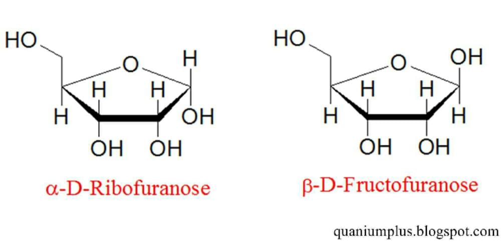
Optical rotations of some compounds along with their structures are given below which of them have D configuration.
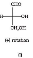
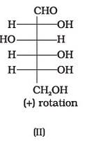
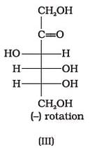
- a)I, II, III
- b)II, III
- c)I, II
- d)III
Correct answer is option 'A'. Can you explain this answer?
Optical rotations of some compounds along with their structures are given below which of them have D configuration.
a)
I, II, III
b)
II, III
c)
I, II
d)
III
|
|
Divey Sethi answered |
The correct answer is Option A.
I, II and III structures have D configuration with -OH group on the lowest asymmetric carbon is on the right side which is comparable to (+) glyceraldehyde.
I, II and III structures have D configuration with -OH group on the lowest asymmetric carbon is on the right side which is comparable to (+) glyceraldehyde.
Which of the following statements is not true about glucose?- a)It is an aldohexose.
- b)On heating with HI it forms n-hexane.
- c)It is present in furanose form.
- d)It does not give 2,4-DNP test.
Correct answer is option 'C'. Can you explain this answer?
Which of the following statements is not true about glucose?
a)
It is an aldohexose.
b)
On heating with HI it forms n-hexane.
c)
It is present in furanose form.
d)
It does not give 2,4-DNP test.
|
|
Prashanth Banerjee answered |
Glucose is present in pyranose form, i.e., five-membered ring structure. Thus, option (iii) is correct because the given statement is incorrect.
Glucose is a monosaccharide that is composed of six carbon atoms with an aldehyde group. Thus, it is an aldohexose. So, this statement is true and therefore, option (i) is incorrect.
Option (ii) is incorrect because the given statement is true. On heating glucose with HI, it forms n-hexane. This reaction suggests that all the six carbon atoms in glucose are linked in a straight chain.
Option (iv) is incorrect because the given statement is true. The aldehyde group is not free in the cyclic structure. So, it does not give 2, 4-DNP test.
What is the primary aim of bioprospecting?- a)To promote sustainable agriculture.
- b)To explore molecular and genetic diversity for economic benefits.
- c)To preserve the traditional knowledge of indigenous peoples.
- d)To breed new hybrid plant species.
Correct answer is option 'B'. Can you explain this answer?
a)
To promote sustainable agriculture.
b)
To explore molecular and genetic diversity for economic benefits.
c)
To preserve the traditional knowledge of indigenous peoples.
d)
To breed new hybrid plant species.

|
Stepway Academy answered |
Bioprospecting involves exploring molecular, genetic, and species-level diversity to discover new products of economic importance, such as medicinal compounds, from natural organisms.
Each polypeptide in a protein has amino acids linked with each other in a specific sequence. This sequence of amino acids is said to be ____________.- a)primary structure of proteins.
- b)secondary structure of proteins.
- c)tertiary structure of proteins.
- d)quaternary structure of proteins.
Correct answer is option 'A'. Can you explain this answer?
Each polypeptide in a protein has amino acids linked with each other in a specific sequence. This sequence of amino acids is said to be ____________.
a)
primary structure of proteins.
b)
secondary structure of proteins.
c)
tertiary structure of proteins.
d)
quaternary structure of proteins.

|
Ameya Basu answered |
The primary structure of a protein refers to the sequence of amino acids in the polypeptide chain. The primary structure is held together by peptide bonds that are made during the process ofprotein biosynthesis.
In the middle of the depletion layer of a reverse biased p-n-junction, the
- a)potential is maximum
- b)electric field is maximum
- c)electric field is zero
- d)potential is zero
Correct answer is option 'C'. Can you explain this answer?
In the middle of the depletion layer of a reverse biased p-n-junction, the
a)
potential is maximum
b)
electric field is maximum
c)
electric field is zero
d)
potential is zero
|
|
Vijay Bansal answered |
Due to the reverse biasing the width of depletion region increases and current flowing through the diode is almost zero. In this case electric field is almost zero at the middle of the depletion region.
Hole is a vacancy or lack of an electron and can travel through the semiconductor material. It can- a)Responsible for current carrier in semicondustor
- b)Move only if an electron stops
- c)Only serves as a vacant spot and cannot conduct current
- d)None of these
Correct answer is option 'A'. Can you explain this answer?
Hole is a vacancy or lack of an electron and can travel through the semiconductor material. It can
a)
Responsible for current carrier in semicondustor
b)
Move only if an electron stops
c)
Only serves as a vacant spot and cannot conduct current
d)
None of these

|
Sai Chakraborty answered |
Explanation:Holes and electrons are the two types of charge carriers responsible for current in semiconductor materials.Holes in a metal or semiconductor crystal lattice can move through the lattice as electrons can, and act similarly to positively-charged particles. They play an important role in the operation of semiconductor devices such as transistors, diodes and integrated circuits. However they are not actually particles, but rather quasiparticles; they are different from the positron, which is the antiparticle of the electron.
In a pure, or intrinsic, semiconductor, valence band holes and conduction-band electrons are always present- a)such that number of holes is greater than the number of electrons
- b)in equal numbers
- c)such that number of electrons is greater than the number of holes
- d)none of these
Correct answer is option 'B'. Can you explain this answer?
In a pure, or intrinsic, semiconductor, valence band holes and conduction-band electrons are always present
a)
such that number of holes is greater than the number of electrons
b)
in equal numbers
c)
such that number of electrons is greater than the number of holes
d)
none of these

|
Sinjini Tiwari answered |
Explanation:An intrinsic semiconductor, also called an undoped semiconductor or i-type semiconductor, is a pure semiconductor without any significant dopant species present. The number of charge carriers is therefore determined by the properties of the material itself instead of the amount of impurities. In intrinsic semiconductors the number of excited electrons and the number of holes are equal: n = p.
What is the significance of the regression slope in the species-area relationship?- a)It represents the rate of species extinction.
- b)It indicates how species richness changes with increasing habitat area.
- c)It determines the biodiversity of tropical regions.
- d)It shows the diversity between plant and animal species.
Correct answer is option 'B'. Can you explain this answer?
a)
It represents the rate of species extinction.
b)
It indicates how species richness changes with increasing habitat area.
c)
It determines the biodiversity of tropical regions.
d)
It shows the diversity between plant and animal species.
|
|
Amar Mehra answered |
Understanding the Species-Area Relationship
The species-area relationship is a fundamental ecological concept that describes how the number of species (species richness) increases with the area of habitat available.
Significance of the Regression Slope
The regression slope in this relationship is crucial because:
- Indicates Change in Species Richness: The slope quantifies how species richness changes as habitat area increases. A steeper slope implies that a larger area supports a disproportionately higher number of species.
- Ecological Insight: This relationship is pivotal for understanding biodiversity patterns. It shows that larger habitats tend to have more species, which is vital for conservation efforts.
- Habitat Fragmentation: The slope can also reflect the impacts of habitat fragmentation, as smaller, isolated areas may support fewer species compared to larger, connected habitats.
Implications for Conservation
- Biodiversity Preservation: Understanding how species richness correlates with area can help in designing reserves and parks to maximize biodiversity.
- Predicting Extinctions: The slope can also aid in predicting potential extinctions as habitats are lost or altered, making it a critical tool for environmental management.
Conclusion
Thus, the regression slope in the species-area relationship is essential for revealing how the number of species changes with increasing habitat area, which is option 'B'. This understanding is vital for effective conservation strategies and maintaining biodiversity in ecosystems.
Nucleic acids are the polymers of ______________.- a)Nucleosides
- b)Nucleotides
- c)Bases
- d)Sugars
Correct answer is option 'B'. Can you explain this answer?
Nucleic acids are the polymers of ______________.
a)
Nucleosides
b)
Nucleotides
c)
Bases
d)
Sugars

|
Amar Pillai answered |
Nucleotides are organic molecules that serve as the monomer units for forming the nucleic acid polymers deoxyribonucleic acid and ribonucleic acid, both of which are essential biomolecules within all life-forms on Earth.
Which of the following is a function of pollinators in ecosystems?- a)To regulate the temperature of the environment.
- b)To control pest populations.
- c)To help in plant reproduction by pollinating flowers.
- d)To filter water and regulate its flow.
Correct answer is option 'C'. Can you explain this answer?
a)
To regulate the temperature of the environment.
b)
To control pest populations.
c)
To help in plant reproduction by pollinating flowers.
d)
To filter water and regulate its flow.

|
Ambition Institute answered |
Pollinators, such as bees, birds, and bats, are crucial for plant reproduction by transferring pollen between flowers, facilitating the fertilization process and enabling the production of fruits and seeds.
Sucrose (cane sugar) is a disaccharide. One molecule of sucrose on hydrolysis gives _________.- a)2 molecules of glucose
- b)2 molecules of glucose + 1 molecule of fructose
- c)1 molecule of glucose + 1 molecule of fructose
- d)2 molecules of fructose
Correct answer is option 'C'. Can you explain this answer?
Sucrose (cane sugar) is a disaccharide. One molecule of sucrose on hydrolysis gives _________.
a)
2 molecules of glucose
b)
2 molecules of glucose + 1 molecule of fructose
c)
1 molecule of glucose + 1 molecule of fructose
d)
2 molecules of fructose

|
Legend S S answered |
A dissacharide on hydrolysis gives two monosaccharides.On hydrolysis of sucrose(cane sugar),equal amounts of glucose and fructose are obtained.
Which of the following is NOT a major cause of species loss?- a)Habitat loss and fragmentation.
- b)Over-exploitation of resources.
- c)Biological invasions.
- d)Increased species-area relationship.
Correct answer is option 'D'. Can you explain this answer?
a)
Habitat loss and fragmentation.
b)
Over-exploitation of resources.
c)
Biological invasions.
d)
Increased species-area relationship.

|
Infinity Academy answered |
The species-area relationship explains how species richness increases with habitat area, but it is not a cause of species loss. The main causes of species loss include habitat loss, over-exploitation, and biological invasions.
The number of valence electrons in a good conductor is generally- a)six or more than six
- b)four
- c)five
- d)three or less than three
Correct answer is option 'D'. Can you explain this answer?
The number of valence electrons in a good conductor is generally
a)
six or more than six
b)
four
c)
five
d)
three or less than three

|
Rishika Chauhan answered |
Explanation:The electron theory states that all matter is composed of atoms and the atoms are composed of smaller particles called protons, electrons, and neutrons. The electrons orbit the nucleus which contains the protons and neutrons. It is the valence electrons that we are most concerned with in electricity. These are the electrons which are easiest to break loose from their parent atom. Normally, conductors have three or less valence electrons; insulators have five or more valence electrons; and semiconductors usually have four valence electrons.
The depletion layer in the p-n junction is caused- a)drift of electrons
- b)drift of holes
- c)migration of impurity ions
- d)diffusion of carrier ions
Correct answer is option 'D'. Can you explain this answer?
The depletion layer in the p-n junction is caused
a)
drift of electrons
b)
drift of holes
c)
migration of impurity ions
d)
diffusion of carrier ions
|
|
Madhurima Mishra answered |
Depletion Layer in the p-n Junction
The p-n junction is a key component in various electronic devices such as diodes and transistors. It is formed by bringing together a p-type semiconductor (which has an excess of holes) and an n-type semiconductor (which has an excess of electrons). When these two materials are joined, a depletion layer is formed at the interface between them.
The depletion layer is a region in the p-n junction where there are no free charge carriers (electrons or holes). It is caused by a combination of diffusion and electric field effects. The depletion layer plays a crucial role in the operation of the p-n junction.
Diffusion of Carrier Ions
One of the main factors contributing to the formation of the depletion layer is the diffusion of carrier ions. In the p-type region, where there is an excess of holes, some of these holes will diffuse across the junction into the n-type region. Similarly, in the n-type region, some of the excess electrons will diffuse into the p-type region.
This diffusion process continues until an equilibrium is reached, where the concentration of carrier ions is equal on both sides of the junction. As a result, a region is formed near the junction that is depleted of carriers, hence the name "depletion layer."
Electric Field Effects
In addition to diffusion, the formation of the depletion layer is also influenced by electric field effects. When the p-n junction is formed, the excess holes in the p-region and excess electrons in the n-region create an electric field that opposes further diffusion of carriers.
This electric field acts as a barrier to the diffusion of holes from the p-region to the n-region and electrons from the n-region to the p-region. As a result, the depletion layer widens and the electric field strength increases, creating a potential barrier that prevents the flow of current in the absence of an external bias.
Conclusion
In summary, the depletion layer in the p-n junction is primarily caused by the diffusion of carrier ions. The excess carriers in the p-type and n-type regions diffuse across the junction, leading to the formation of a region depleted of carriers. The electric field effects also contribute to the widening of the depletion layer by opposing further carrier diffusion. Understanding the formation and characteristics of the depletion layer is essential in analyzing the behavior and functionality of p-n junction devices.
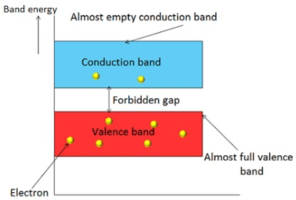
The main difference between conductors, semiconductors and insulators is because of- a)Work function
- b)Mobility of electrons
- c)Energy of electrons
- d)Width of forbidden energy gap
Correct answer is option 'D'. Can you explain this answer?
The main difference between conductors, semiconductors and insulators is because of
a)
Work function
b)
Mobility of electrons
c)
Energy of electrons
d)
Width of forbidden energy gap

|
Niti Saha answered |
Explanation:Forbidden gap plays a major role for determining the electrical conductivity of material. Based on the forbidden gap materials are classified in to three types, they are : Insulators : The forbidden gap between the valence band and conduction band is very large in insulators. The energy gap of insulator is approximately equal to 15 electron volts (eV).Conductors: In a conductor, valence band and conduction band overlap each other. Therefore, there is no forbidden gap in a conductor.Semiconductors: In semiconductors, the forbidden gap between valence band and conduction band is very small. It has a forbidden gap of about 1 electron volt (eV).
A p- type semiconductor can be obtained by adding- a)gallium to pure silicon
- b)phosphorus to pure germanium
- c)arsenic to pure silicon
- d)antimony to pure germanium
Correct answer is option 'A'. Can you explain this answer?
A p- type semiconductor can be obtained by adding
a)
gallium to pure silicon
b)
phosphorus to pure germanium
c)
arsenic to pure silicon
d)
antimony to pure germanium

|
Gauri Sharma answered |
Explanation:In P-type doping, boron or gallium is the dopant. Boron and gallium each have only three outer electrons. When mixed into the silicon lattice, they form "holes" in the lattice where a silicon electron has nothing to bond to. The absence of an electron creates the effect of a positive charge, hence the name P-type.Holes can conduct current. A hole happily accepts an electron from a neighbor, moving the hole over a space. P-type silicon is a good conductor.
In the case of metals the valence and conduction bands have- a)no overlap, energy gap is large
- b)no overlap, energy gap is small
- c)overlap, energy gap =0
- d)no overlap, energy gap =0
Correct answer is option 'C'. Can you explain this answer?
In the case of metals the valence and conduction bands have
a)
no overlap, energy gap is large
b)
no overlap, energy gap is small
c)
overlap, energy gap =0
d)
no overlap, energy gap =0

|
Yash Kumar answered |
Explanation:
In the case of metals, the valence and conduction bands have an overlap, and the energy gap between them is zero.
1. Valence Band:
- The valence band is the highest energy band that is fully occupied by electrons in a material at absolute zero temperature.
- It consists of the valence electrons, which are tightly bound to the atomic nuclei.
- These electrons are not free to move and contribute to the electrical conductivity of the material.
2. Conduction Band:
- The conduction band is the energy band located just above the valence band.
- It contains empty or partially filled energy states that are available for electrons to move freely and contribute to the electrical conductivity of the material.
- Electrons in the conduction band have higher energy and are not bound to any specific atom.
3. Energy Gap:
- The energy gap is the energy difference between the valence and conduction bands.
- In insulators, this gap is large, typically on the order of several electron volts, which makes it difficult for electrons to move from the valence band to the conduction band.
- In semiconductors, the energy gap is smaller than in insulators, allowing some electrons to acquire enough energy to move from the valence band to the conduction band, contributing to electrical conductivity.
- In metals, the energy gap between the valence and conduction bands is zero, meaning that there is no energy barrier for electrons to move from the valence band to the conduction band.
- This overlap allows electrons to move freely throughout the material, resulting in high electrical conductivity.
Conclusion:
In summary, in the case of metals, the valence and conduction bands have an overlap, and the energy gap between them is zero. This overlap allows electrons to move freely, contributing to the high electrical conductivity observed in metals.
DNA and RNA contain four bases each. Which of the following bases is not present in RNA?- a)Adenine
- b)Uracil
- c)Thymine
- d)Cytosine
Correct answer is option 'C'. Can you explain this answer?
DNA and RNA contain four bases each. Which of the following bases is not present in RNA?
a)
Adenine
b)
Uracil
c)
Thymine
d)
Cytosine

|
Rahul Desai answered |
Thymine is one of the four nucleobases in the nucleic acid of DNA that are represented by the letters G–C–A–T. The others are adenine, guanine, and cytosine. Thymine is also known as 5-methyluracil, a pyrimidine nucleobase. In RNA, thymine is replaced by the nucleobase uracil.
Which of the following reactions of glucose can be explained only by its cyclic structure?- a)Glucose forms pentaacetate.
- b)Glucose reacts with hydroxylamine to form an oxime.
- c)Pentaacetate of glucose does not react with hydroxylamine.
- d)Glucose is oxidised by nitric acid to gluconic acid.
Correct answer is option 'C'. Can you explain this answer?
Which of the following reactions of glucose can be explained only by its cyclic structure?
a)
Glucose forms pentaacetate.
b)
Glucose reacts with hydroxylamine to form an oxime.
c)
Pentaacetate of glucose does not react with hydroxylamine.
d)
Glucose is oxidised by nitric acid to gluconic acid.

|
Anoushka Chopra answered |
The pentaacetate of glucose does not react with hydroxylamine. This indicates that the aldehyde in glucose is not free and is involved in the formation of cyclic structure. Hence, this reaction of glucose can only be explained by its cyclic structure. Thus, option (iii) is correct.
Option (i) is incorrect because the capability of glucose to form pentaacetate tells us about the 5 hydroxyl group of the glucose.
Option (ii) is incorrect because this reaction confirms the presence of a carbonyl group in glucose.
Option (iv) is incorrect because this reaction indicates the presence of a primary alcohol in the glucose.
The output from a full wave rectifier is- a)a pulsating unidirectional voltage
- b)a pulsating dc voltage
- c)zero
- d)none
Correct answer is option 'A'. Can you explain this answer?
The output from a full wave rectifier is
a)
a pulsating unidirectional voltage
b)
a pulsating dc voltage
c)
zero
d)
none

|
Ciel Knowledge answered |
The output from a full wave rectifier is a pulsating unidirectional voltage. This is because while the rectifier converts AC to DC, the output is not a pure DC voltage; it contains fluctuations due to the rectification process. These fluctuations make the output a pulsating DC, which is unidirectional. To achieve a steady DC output, additional filtering components like capacitors are often used to smooth out the voltage.
A piece of copper and another of germanium are cooled from room temperature to 80 K. The resistance of- a)copper decreases and that of germanium increases
- b)each of them increases
- c)each of them decreases
- d)copper increases and that of germanium decreases
Correct answer is option 'A'. Can you explain this answer?
A piece of copper and another of germanium are cooled from room temperature to 80 K. The resistance of
a)
copper decreases and that of germanium increases
b)
each of them increases
c)
each of them decreases
d)
copper increases and that of germanium decreases
|
|
Geetika Tiwari answered |
We know, a piece of copper is a metal while that of germanium is a semiconducting material. For metals resistance increases with increase in temperature. The semiconductor has a negative temperature coefficient of resistance. Hence, when it is cooled its resistance increases.
Motion of hole is a convenient way of describing- a)the actual motion of bound electrons
- b)the actual motion of energy gap
- c)the actual motion of free electrons
- d)the actual motion of conduction electrons
Correct answer is option 'A'. Can you explain this answer?
Motion of hole is a convenient way of describing
a)
the actual motion of bound electrons
b)
the actual motion of energy gap
c)
the actual motion of free electrons
d)
the actual motion of conduction electrons

|
Anjali Reddy answered |
Explanation:The holes are just the abscence of a electron in a energy band. But its easier to describe the abscence of a electron as a single moving positive charge than it is to describe the motion of all the other electrons in the band.In a band you have N electrons. Remove one of those electrons(by for instance p-doping) and you have N-1 electrons left. Now you can either choose to describe this with the behavior of those N-1 electrons. Or you can choose to describe it as if there is one single hole moving around in the band.So mathematicly the holes behave just like a positivly charged electron.
Proteins are found to have two different types of secondary structures viz. α-helix and β-pleated sheet structure. α-helix structure of protein is stabilised by :- a)Peptide bonds
- b)van der Waals forces
- c)Hydrogen bonds
- d)Dipole-dipole interactions
Correct answer is option 'C'. Can you explain this answer?
Proteins are found to have two different types of secondary structures viz. α-helix and β-pleated sheet structure. α-helix structure of protein is stabilised by :
a)
Peptide bonds
b)
van der Waals forces
c)
Hydrogen bonds
d)
Dipole-dipole interactions
|
|
Rahul Desai answered |
In α-helix, hydrogen bonds are present between –NH group of one amino acid residue to the >C= O group of another aminoacid residue.
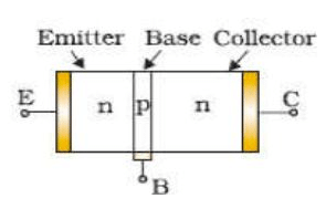
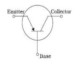
In an N-P-N transistor, P-type crystal is- a)collector
- b)base
- c)grid
- d)emitter
Correct answer is option 'B'. Can you explain this answer?
In an N-P-N transistor, P-type crystal is
a)
collector
b)
base
c)
grid
d)
emitter

|
Gauri Khanna answered |
Explanation:When the p-type crystal is grown between relatively wide sections of n-type crystals then the transistor is called NPN transistor.
In a semiconductor, the forbidden energy gap between the valance band and the conduction band is of the order of- a)1 ev
- b)1 MeV
- c)5 eV
- d)1 GeV
Correct answer is option 'A'. Can you explain this answer?
In a semiconductor, the forbidden energy gap between the valance band and the conduction band is of the order of
a)
1 ev
b)
1 MeV
c)
5 eV
d)
1 GeV

|
Sankar Gupta answered |
Explanation:The material which has electrical conductivity between that of a conductor and an insulator is called as semiconductor. Silicon, germanium and graphite are some examples of semiconductors.
In semiconductors, the forbidden gap between valence band and conduction band is very small. It has a forbidden gap of about 1 electron volt (eV).
Electrons are forbidden in a band (in a crystal) called the- a)valence band
- b)forbidden band
- c)conduction band
- d)memory band
Correct answer is option 'B'. Can you explain this answer?
Electrons are forbidden in a band (in a crystal) called the
a)
valence band
b)
forbidden band
c)
conduction band
d)
memory band
|
|
Sinjini Tiwari answered |
Explanation:A region of values of energy that electrons in an ideal crystal (without defects) cannot have. In semiconductors the forbidden band separating the valence band and the conduction band is usually considered. In this case the energy difference between the lower level (bottom) of the conduction band and the upper level (ceiling) of the valence band is called the width of the forbidden band.
Depletion region (space charge) is formed because- a)majority carriers while diffusing to the other side leave behind immobile ionized atoms
- b)majority carriers while drifting to the other side leave behind immobile ionized atoms
- c)majority carriers while diffusing to the other side leave behind highly mobile ionized atoms
- d)minority carriers while diffusing to the other side leave behind immobile ionized atoms
Correct answer is option 'A'. Can you explain this answer?
Depletion region (space charge) is formed because
a)
majority carriers while diffusing to the other side leave behind immobile ionized atoms
b)
majority carriers while drifting to the other side leave behind immobile ionized atoms
c)
majority carriers while diffusing to the other side leave behind highly mobile ionized atoms
d)
minority carriers while diffusing to the other side leave behind immobile ionized atoms

|
Kunal Pillai answered |
Depletion region (space charge) is formed because majority carriers while diffusing to the other side leave behind immobile ionized atoms.
Explanation:
The depletion region, also known as the space charge region, is a region within a semiconductor device where there are no mobile charge carriers. This region is formed as a result of the movement of majority carriers (electrons in N-type material and holes in P-type material) across the junction between the N and P-type regions of a semiconductor.
When a P-N junction is formed, the N-type region has an excess of electrons and the P-type region has a deficit of electrons (excess of holes). When the two regions are brought together, the majority carriers (electrons or holes) will start to diffuse across the junction due to the concentration gradient. However, as they move across the junction, they will encounter dopant atoms of the opposite type (N-type carriers encountering P-type dopants and vice versa).
The majority carriers that diffuse across the junction will either recombine with the majority carriers of the opposite type or they will ionize the dopant atoms. In the case of ionization, the majority carriers will give up their energy to the dopant atoms, causing them to become immobile ions. These immobile ions create a region within the semiconductor where there are no mobile charge carriers, known as the depletion region.
The depletion region is characterized by a fixed electric field, which acts as a barrier to the flow of majority carriers. This creates a potential difference across the junction, known as the built-in potential. The presence of the depletion region and the built-in potential are essential for the functioning of semiconductor devices such as diodes and transistors.
In summary, the depletion region is formed because majority carriers, while diffusing to the other side of a P-N junction, leave behind immobile ionized atoms. These immobile ions create a region within the semiconductor where there are no mobile charge carriers, resulting in the formation of the depletion region.
Majority current carriers in N – types are- a)holes
- b)negative ions
- c)positive ions
- d)electrons
Correct answer is option 'D'. Can you explain this answer?
Majority current carriers in N – types are
a)
holes
b)
negative ions
c)
positive ions
d)
electrons
|
|
Anjali Reddy answered |
Explanation:The more abundant charge carriers are called majority carriers, which are primarily responsible for current transport in a piece of semiconductor. In n-type semiconductors they are electrons, while in p-type semiconductors they are holes.
When n –type of semiconductor is heated- a)number of electrons increases while that of holes decreases
- b)number of electrons and holes increases equally
- c)number of holes increases while that of electrons is same
- d)number of electrons and holes remains same
Correct answer is option 'B'. Can you explain this answer?
When n –type of semiconductor is heated
a)
number of electrons increases while that of holes decreases
b)
number of electrons and holes increases equally
c)
number of holes increases while that of electrons is same
d)
number of electrons and holes remains same
|
|
Gauri Khanna answered |
Explanation:Due to heating, when a free electron is produced then simultaneously a hole is also produced.
When the conductivity of a semiconductor is only due to breaking of the covalent bonds, the semiconductor is called- a)donor
- b)acceptor
- c)intrinsic
- d)extrinsic
Correct answer is option 'C'. Can you explain this answer?
When the conductivity of a semiconductor is only due to breaking of the covalent bonds, the semiconductor is called
a)
donor
b)
acceptor
c)
intrinsic
d)
extrinsic

|
Arpita Nair answered |
Explanation:A pure semiconductor is called intrinsic semiconductor, e.g., silicon, germanium. The presence of the mobile charge carriers is the intrinsic property of the material. At room temperature, some covalent bonds are broken and electrons are made free. The absence of electron in the covalent bond form hole.The electrical conduction is by means of mobile electrons and holes. Hole act as positive charge, because it can attract an electron. If some other bond is broken and the electron thus freed fills this hole(vacancy), it seems as though the hole is moving.Actually an electron is travelling in opposite direction. In a pure(intrinsic) semiconductor, the number of holes is equal to the number of free electrons.
Chapter doubts & questions for February Week 3 - Weekly Tests for NEET Preparation 2025 is part of NEET exam preparation. The chapters have been prepared according to the NEET exam syllabus. The Chapter doubts & questions, notes, tests & MCQs are made for NEET 2025 Exam. Find important definitions, questions, notes, meanings, examples, exercises, MCQs and online tests here.
Chapter doubts & questions of February Week 3 - Weekly Tests for NEET Preparation in English & Hindi are available as part of NEET exam.
Download more important topics, notes, lectures and mock test series for NEET Exam by signing up for free.
|
© EduRev
|
Education Revolution
|


|


Signup to see your scores
go up within 7 days!
Access 1000+ FREE Docs, Videos and Tests
Takes less than 10 seconds to signup