


All Exams > Electrical Engineering (EE) > Topicwise Question Bank for Electrical Engineering > All Questions
All questions of Analog Electronics for Electrical Engineering (EE) Exam
Req = ?
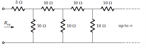
- a)11.86 ohm
- b)10 ohm
- c)25 ohm
- d)11.18 ohm
Correct answer is option 'D'. Can you explain this answer?
Req = ?
a)
11.86 ohm
b)
10 ohm
c)
25 ohm
d)
11.18 ohm
| | Ravi Singh answered |
- Req – 5 = 10(Req + 5)/(10 + 5 +Req).
- Solving for Req we have
Req = 11.18 ohm.

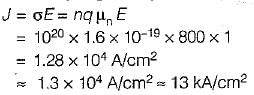
The density and mobility of electrons in a conductor are respectively 1020/cm3 and 800 cm2/V-s. If a uniform electric field of 1 V/cm exists across this conductor, then the electron current density would be approximately- a)11 kA/cm2
- b)9 kA/cm2
- c)13 kA/cm2
- d)18 kA/cm2
Correct answer is option 'C'. Can you explain this answer?
The density and mobility of electrons in a conductor are respectively 1020/cm3 and 800 cm2/V-s. If a uniform electric field of 1 V/cm exists across this conductor, then the electron current density would be approximately
a)
11 kA/cm2
b)
9 kA/cm2
c)
13 kA/cm2
d)
18 kA/cm2
 | Pioneer Academy answered |
The current density is given by
A solid copper sphere, 10 cm in diameter is deprived of 1020 electrons by a charging scheme. The charge on the sphere is- a)160.2 C
- b)-160.2 C
- c)16.02 C
- d)-16.02 C
Correct answer is option 'C'. Can you explain this answer?
A solid copper sphere, 10 cm in diameter is deprived of 1020 electrons by a charging scheme. The charge on the sphere is
a)
160.2 C
b)
-160.2 C
c)
16.02 C
d)
-16.02 C
| | Aditya Deshmukh answered |
n 10^20, Q = ne = e 10^20 = 16.02 C.
Charge on sphere will be positive.
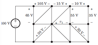
Consider the circuit graph shown in figure below. Each branch of circuit graph represent a circuit element. The value of voltage V1 is
- a)30 V
- b)25 V
- c)20 V
- d)15 V
Correct answer is option 'D'. Can you explain this answer?
Consider the circuit graph shown in figure below. Each branch of circuit graph represent a circuit element. The value of voltage V1 is
a)
30 V
b)
25 V
c)
20 V
d)
15 V
 | Gate Gurus answered |
- 100 = 65 + V2 ⇒ V2 = 35 V
- V3 – 30 = V2 ⇒ V3 = 65 V
- 105 – V3 + V4 – 65 = 0 ⇒ V4 = 25 V
- V4 + 15 – 55 + V1 = 0 ⇒ V1 = 15 V.
With the increase in temperature, the resistivity of an intrinsic semiconductor decreases. This is because, with the increase of temperature- a)the carrier concentration decreases, but the mobility of carriers increases.
- b)the carrier concentration increases, but the mobility of carriers decreases.
- c)the carrier concentration remains the same but the mobility of carriers decreases.
- d)both the carrier concentration and mobility of carriers decreases
Correct answer is option 'B'. Can you explain this answer?
With the increase in temperature, the resistivity of an intrinsic semiconductor decreases. This is because, with the increase of temperature
a)
the carrier concentration decreases, but the mobility of carriers increases.
b)
the carrier concentration increases, but the mobility of carriers decreases.
c)
the carrier concentration remains the same but the mobility of carriers decreases.
d)
both the carrier concentration and mobility of carriers decreases
| | Malavika Nair answered |
In an intrinsic semiconductor, as the temperature increases mobility is slightly reduced since mobility of charge carrier is inversely proportional to temperature. This will slightly reduce the conductivity. But, due to temperature effect, large number of covalent bonds are broken which creates electrons and holes and this increases the conductivity by a larger value. As a result of this resistivity is decreased 
If a current of 1.6 μA is flowing through a conductor, the number of electrons crossing a particular cross-section per second will be- a)1013
- b)1.6
- c)1019
- d)1.6 x 10⁻⁶
Correct answer is option 'A'. Can you explain this answer?
If a current of 1.6 μA is flowing through a conductor, the number of electrons crossing a particular cross-section per second will be
a)
1013
b)
1.6
c)
1019
d)
1.6 x 10⁻⁶
| | Lavanya Menon answered |
Given, I = 1.6 x 10⁻⁶ A
= 1.6 x 10⁻⁶ Coulomb/second
Charge crossing a particular cross-section per second = 1.6 x 10⁻⁶ C Hence, number of electrons crossing a particular cross-section per second
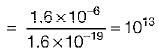
= 1.6 x 10⁻⁶ Coulomb/second
Charge crossing a particular cross-section per second = 1.6 x 10⁻⁶ C Hence, number of electrons crossing a particular cross-section per second
The energy required to charge a 10 µF capacitor to 100 V is- a)0.1 J
- b)0.05 J
- c) 5 x 10(-9) J
- d)10 x 10(-9) J
Correct answer is option 'B'. Can you explain this answer?
The energy required to charge a 10 µF capacitor to 100 V is
a)
0.1 J
b)
0.05 J
c)
5 x 10(-9) J
d)
10 x 10(-9) J
| | Sanjana Chopra answered |
Energy provided is equal to 0.5 CVxV.

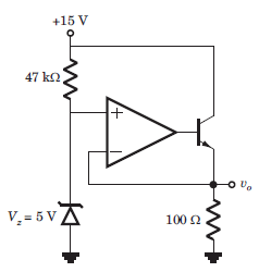
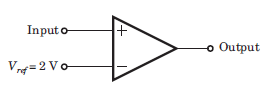
The LED in the circuit of fig. will be on if vi is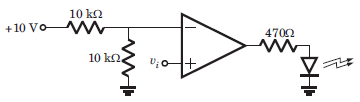
- a) > 10 V
- b)<10 V
- c) > 5 V
- d)< 5 V
Correct answer is option 'C'. Can you explain this answer?
The LED in the circuit of fig. will be on if vi is
a)
> 10 V
b)
<10 V
c)
> 5 V
d)
< 5 V
| | Anjana Khatri answered |
When v+ > 5 V, output will be positive and LED will be on. Hence (C) is correct.
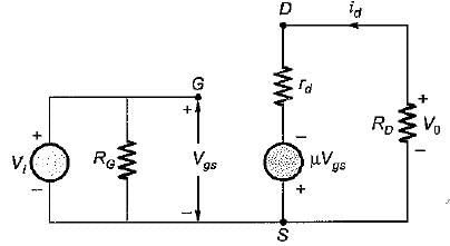
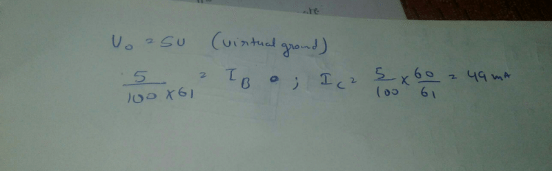
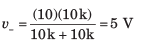
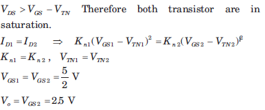
Consider the circuit shown in fig.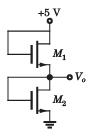 The both transistor have parameter as followsVTN = 0.8V, kn' = 30 μA/V2Que: If the width-to-length ratios of M1 and M2 are(W/L)1 = (W/L)2 = 40The output Vo is
- a)2.5 V
- b)2.5 V
- c)5 V
- d)0 V
Correct answer is option 'B'. Can you explain this answer?
Consider the circuit shown in fig.
The both transistor have parameter as follows
VTN = 0.8V, kn' = 30 μA/V2
Que: If the width-to-length ratios of M1 and M2 are
(W/L)1 = (W/L)2 = 40
The output Vo is
a)
2.5 V
b)
2.5 V
c)
5 V
d)
0 V
| | Sanvi Kapoor answered |
For both transistor VDS = VGS ,
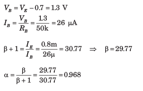
In an n-p-n transistor biased in the active region, as the magnitude of the collector-base voltage is increased,- a)the base current increases because more electrons are injected from the emitter.
- b)the base current increases because more holes are injected from the base to the collector.
- c)the emitter current decreases because the base-emitter junction gets slightly less forward biased.
- d)the collector current increases slightly because the base width reduces.
Correct answer is option 'D'. Can you explain this answer?
In an n-p-n transistor biased in the active region, as the magnitude of the collector-base voltage is increased,
a)
the base current increases because more electrons are injected from the emitter.
b)
the base current increases because more holes are injected from the base to the collector.
c)
the emitter current decreases because the base-emitter junction gets slightly less forward biased.
d)
the collector current increases slightly because the base width reduces.
| | Mahesh Datta answered |
IC increases because base width reduces due to early effect.
Consider a voltage series feedback network, where amplifier gain = 100, feedback factor = 5. For the basic amplifier, input voltage = 4V, input current=2mA. Find the input resistance of the network.- a)1.002kΩ
- b)1002kΩ
- c)2kΩ
- d)2000kΩ
Correct answer is option 'B'. Can you explain this answer?
Consider a voltage series feedback network, where amplifier gain = 100, feedback factor = 5. For the basic amplifier, input voltage = 4V, input current=2mA. Find the input resistance of the network.
a)
1.002kΩ
b)
1002kΩ
c)
2kΩ
d)
2000kΩ
 | Athul Das answered |
To find the input resistance of the network, we can use the formula:
Input resistance (Rin) = (Voltage gain / Current gain) * (Feedback factor / Amplifier gain)
Given:
Amplifier gain (Av) = 100
Feedback factor (β) = 5
The voltage gain (Av) can be calculated as the ratio of output voltage (Vo) to input voltage (Vi):
Av = Vo / Vi
Since it is a voltage series feedback network, the output voltage (Vo) and input voltage (Vi) are related by the formula:
Vo = Vi / (1 + β * Av)
Substituting the given values:
Av = 100
β = 5
Vo = Vi / (1 + 5 * 100)
Vo = Vi / 501
Now, we can calculate the output voltage (Vo) using the formula:
Vo = Av * Vi
Vo = 100 * 4V
Vo = 400V
Substituting the calculated values into the equation for Vo:
400V = Vi / 501
Solving for Vi:
Vi = 400V * 501
Vi = 200,400V
Now, we can substitute the calculated values into the formula for input resistance (Rin):
Rin = (Av / Ai) * (β / Av)
Rin = (100 / (2mA / 200,400V)) * (5 / 100)
Rin = (100 / (0.002A / 200,400V)) * (5 / 100)
Rin = (100 / (0.002A / 200,400V)) * (5 / 100)
Rin = (100 / (0.002A / 200,400V)) * (5 / 100)
Rin = (100 / 0.002A) * (5 / 100)
Rin = (100 / 0.002A) * (5 / 100)
Rin = (100 / 0.002A) * (5 / 100)
Rin = (100 / 0.002A) * (5 / 100)
Rin = (100 / 0.002A) * (5 / 100)
Rin = 1,000 * 0.05
Rin = 50
Therefore, the input resistance of the network is 50 ohms.
Assertion (A): The drift velocity is in the direction opposite to that of the electric field.
Reason (R): At each inelastic collision with an ion, an electron loses energy, and a steady-state condition is reached where a finite value of drift speed is attained.- a)Both A and R are true and R is the correct explanation of A.
- b)Both A and R are true but R is not the correct explanation of A.
- c)A is true but R is false.
- d)A is false but R is true.
Correct answer is option 'B'. Can you explain this answer?
Assertion (A): The drift velocity is in the direction opposite to that of the electric field.
Reason (R): At each inelastic collision with an ion, an electron loses energy, and a steady-state condition is reached where a finite value of drift speed is attained.
Reason (R): At each inelastic collision with an ion, an electron loses energy, and a steady-state condition is reached where a finite value of drift speed is attained.
a)
Both A and R are true and R is the correct explanation of A.
b)
Both A and R are true but R is not the correct explanation of A.
c)
A is true but R is false.
d)
A is false but R is true.
 | Dj Bravo answered |
Both assertion and reason are individually correct statements. However, the reason for assertion is that due to the applied electric field, and electrostatic force is developed on the electron and the electrons would be accelerated in a direction opposite to the applied electric field and this motion is called directed motion of electron
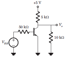
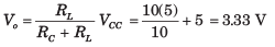
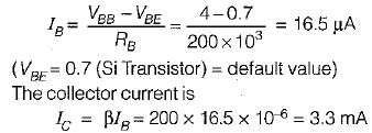
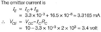
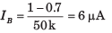
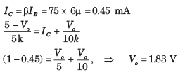
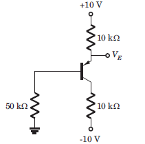
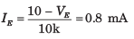
For the circuit shown below, the collector to emitter voltage is
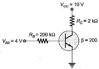
- a)1.25 V
- b)3.40 V
- c)-2.30 V
- d)0 V
Correct answer is option 'B'. Can you explain this answer?
For the circuit shown below, the collector to emitter voltage is
a)
1.25 V
b)
3.40 V
c)
-2.30 V
d)
0 V
| | Sanya Agarwal answered |
Let the transistor be operating under active region.
The theoretical maximum efficiency of a bridge rectifier circuit is- a)48.2%
- b)40.53%
- c)81.06%
- d)82%
Correct answer is option 'C'. Can you explain this answer?
The theoretical maximum efficiency of a bridge rectifier circuit is
a)
48.2%
b)
40.53%
c)
81.06%
d)
82%
| | Sanya Agarwal answered |
For a bridge rectifier circuit,
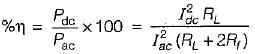
For ideal diode,
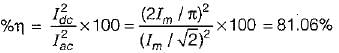
and hence maximum efficiency, η = 81.06%.
For ideal diode,
and hence maximum efficiency, η = 81.06%.


What is the reverse transmission factor?- a)Ratio of output by input signal
- b)Ratio of feedback by input signal
- c)Ration of feedback by output signal
- d)Ratio of input by feedback signal
Correct answer is option 'C'. Can you explain this answer?
What is the reverse transmission factor?
a)
Ratio of output by input signal
b)
Ratio of feedback by input signal
c)
Ration of feedback by output signal
d)
Ratio of input by feedback signal
| | Pooja Patel answered |
In feedback systems, the feedback signal is in proportion with the output signal.
XF ∝ XO
XF = βXO, where β is the feedback factor or reverse transmission factor.
XF ∝ XO
XF = βXO, where β is the feedback factor or reverse transmission factor.
In a feedback network, input voltage is 14V, feedback voltage is 6V and source voltage is 20V. β is in ohms. What is its configuration?- a)Shunt-Shunt feedback
- b)Shunt-Series feedback
- c)Series-Series feedback
- d)Series-Shunt feedback
Correct answer is option 'C'. Can you explain this answer?
In a feedback network, input voltage is 14V, feedback voltage is 6V and source voltage is 20V. β is in ohms. What is its configuration?
a)
Shunt-Shunt feedback
b)
Shunt-Series feedback
c)
Series-Series feedback
d)
Series-Shunt feedback
| | Pioneer Academy answered |
Given that input is 14V, feedback is 6V and source is 20 V, we can see
VI = VS – VF, which is voltage mixing. Also, β is in ohms that is voltage/current.
Since output of feedback is voltage and input is current, the output has current sampling.
Thus, configuration is a series-series feedback/current – series feedback.
VI = VS – VF, which is voltage mixing. Also, β is in ohms that is voltage/current.
Since output of feedback is voltage and input is current, the output has current sampling.
Thus, configuration is a series-series feedback/current – series feedback.
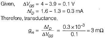
What are the values of VP and ID for VGS = 0.5 V of an N-channel FET that has IDSS = 10 mA with drain voltage of 5 V and gmo = 5 mA/V?- a)2 V and 7.65 mA
- b)4 V and 3.83 mA
- c)4 V and 7.65 mA
- d)2 V and 3.83 mA
Correct answer is option 'C'. Can you explain this answer?
What are the values of VP and ID for VGS = 0.5 V of an N-channel FET that has IDSS = 10 mA with drain voltage of 5 V and gmo = 5 mA/V?
a)
2 V and 7.65 mA
b)
4 V and 3.83 mA
c)
4 V and 7.65 mA
d)
2 V and 3.83 mA
| | Aniket Shah answered |
Given data:
VGS = 0.5 V
IDSS = 10 mA
VDS = 5 V
gmo = 5 mA/V
To find:
Values of VP and ID
- Calculation of VP:
VP can be calculated using the formula:
VP = VGS - ID/2 * (1/gmo)
Given:
VGS = 0.5 V
IDSS = 10 mA
gmo = 5 mA/V
Substituting the values in the formula:
VP = 0.5 V - (10 mA)/(2 * 5 mA/V)
VP = 0.5 V - 1 V
VP = -0.5 V
- Calculation of ID:
ID can be calculated using the formula:
ID = IDSS * (1 - VGS/VP)^2
Given:
VGS = 0.5 V
IDSS = 10 mA
VP = -0.5 V
Substituting the values in the formula:
ID = 10 mA * (1 - 0.5 V / -0.5 V)^2
ID = 10 mA * (1 + 1)^2
ID = 10 mA * 4
ID = 40 mA
Therefore, the values of VP and ID for VGS = 0.5 V are:
VP = -0.5 V
ID = 40 mA
Hence, the correct answer is option C) 4 V and 7.65 mA.
VGS = 0.5 V
IDSS = 10 mA
VDS = 5 V
gmo = 5 mA/V
To find:
Values of VP and ID
- Calculation of VP:
VP can be calculated using the formula:
VP = VGS - ID/2 * (1/gmo)
Given:
VGS = 0.5 V
IDSS = 10 mA
gmo = 5 mA/V
Substituting the values in the formula:
VP = 0.5 V - (10 mA)/(2 * 5 mA/V)
VP = 0.5 V - 1 V
VP = -0.5 V
- Calculation of ID:
ID can be calculated using the formula:
ID = IDSS * (1 - VGS/VP)^2
Given:
VGS = 0.5 V
IDSS = 10 mA
VP = -0.5 V
Substituting the values in the formula:
ID = 10 mA * (1 - 0.5 V / -0.5 V)^2
ID = 10 mA * (1 + 1)^2
ID = 10 mA * 4
ID = 40 mA
Therefore, the values of VP and ID for VGS = 0.5 V are:
VP = -0.5 V
ID = 40 mA
Hence, the correct answer is option C) 4 V and 7.65 mA.
N-channel FETs are superior to P-channel FETs, because- a)they have higher input impedance
- b)mobility of electrons is greater than that of holes
- c)they consume less power
- d)they have high switching speed
Correct answer is option 'B'. Can you explain this answer?
N-channel FETs are superior to P-channel FETs, because
a)
they have higher input impedance
b)
mobility of electrons is greater than that of holes
c)
they consume less power
d)
they have high switching speed
| | Sushant Mehta answered |
n-channel FETs are superior to p-chanel FETs because n-channel FETs are faster than p-channel FETs since μn > μP.
The barrier voltage for germanium is _________ at 25°C.- a)0.6 V
- b)0.1 V
- c)0.3 V
- d)0.5 V
Correct answer is option 'C'. Can you explain this answer?
The barrier voltage for germanium is _________ at 25°C.
a)
0.6 V
b)
0.1 V
c)
0.3 V
d)
0.5 V
| | Sarthak Yadav answered |
The barrier potential of the "Germanium" diode is 0.3 V.
A FET tuned amplifier with gm = 5 mA/V, rd = 20 kΩ has a resonant impedance of 20 kΩ. The gain at resonance is given by- a)200
- b)100
- c)50
- d)25
Correct answer is option 'C'. Can you explain this answer?
A FET tuned amplifier with gm = 5 mA/V, rd = 20 kΩ has a resonant impedance of 20 kΩ. The gain at resonance is given by
a)
200
b)
100
c)
50
d)
25
| | Abhay Khanna answered |
AV = Gain at resonance = gmR
Here, R = rd ║Rmax
∴ AV = 5x 10-3 x 10 x 103 = 50
Here, R = rd ║Rmax
∴ AV = 5x 10-3 x 10 x 103 = 50
If ‘V’ is the voltage phasor and ‘I’ is the current phasor, then VI represents- a)Apparent power
- b)Active power
- c)Reactive power
- d)Total power
Correct answer is option 'A'. Can you explain this answer?
If ‘V’ is the voltage phasor and ‘I’ is the current phasor, then VI represents
a)
Apparent power
b)
Active power
c)
Reactive power
d)
Total power
| | Sarita Yadav answered |
Apparent Power (S): It is defined as the product of r.m.s value of voltage (V) and current (1). It is denoted by S. S = V/I Volt Ampere
The Zener diode VZ1 in the figure shown below has the reverse saturation current of 20 mA and reverse breakdown voltage of 100 V whereas the corresponding values for diode VZ2 are 40 μA and 40 V.
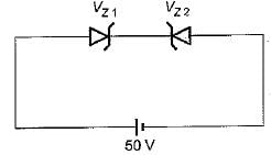 The current through the circuit is
- a)20 μA anticlockwise
- b)20 μA clockwise
- c)40 μA anticlockwise
- d)40 μA clockwise
Correct answer is option 'D'. Can you explain this answer?
The Zener diode VZ1 in the figure shown below has the reverse saturation current of 20 mA and reverse breakdown voltage of 100 V whereas the corresponding values for diode VZ2 are 40 μA and 40 V.
The current through the circuit is
a)
20 μA anticlockwise
b)
20 μA clockwise
c)
40 μA anticlockwise
d)
40 μA clockwise
| | Avik Saha answered |
The Zener diode VZ2 is reverse biased and VZ1 is forward biased. As both Zener diodes \/Z1 and VZ2 are connected in series, the reverse saturation current 40 μA of VZ2 will flow clockwise in the circuit as 50 V reverse bias appears across the VZ2 diode.
What is the value of thermal resistance for the 2N338 transistor for which the manufacturer specifies PC,max = 125 mW at 25°C free-air temperature and maximum junction temperature of 150°C?- a)1.0°C/mW
- b)1.45°C/mW
- c)1.2°C/mW
- d)0.2°C/mW
Correct answer is option 'A'. Can you explain this answer?
What is the value of thermal resistance for the 2N338 transistor for which the manufacturer specifies PC,max = 125 mW at 25°C free-air temperature and maximum junction temperature of 150°C?
a)
1.0°C/mW
b)
1.45°C/mW
c)
1.2°C/mW
d)
0.2°C/mW
| | Avik Saha answered |
Calculating Thermal Resistance for 2N338 Transistor:
In this case, we are given the maximum power dissipation (PC,max) of the 2N338 transistor as 125 mW at a free-air temperature of 25°C and a maximum junction temperature of 150°C. To calculate the thermal resistance of the transistor, we can use the formula:
Thermal Resistance (θ) = (Tj - Ta) / PC,max
Where:
- θ is the thermal resistance
- Tj is the junction temperature (150°C)
- Ta is the ambient temperature (25°C)
- PC,max is the maximum power dissipation (125 mW)
Now, substituting the given values into the formula:
θ = (150°C - 25°C) / 125 mW
θ = 125°C / 125 mW
θ = 1.0 °C/mW
Therefore, the thermal resistance of the 2N338 transistor is 1.0 °C/mW. This means that for every 1 mW of power dissipated by the transistor, the junction temperature will increase by 1.0°C above the ambient temperature.
Assertion (A): An emitter follower is widely used in electronic instruments.
Reason (R): The voltage gain of emitter follower is very high.- a)Both A and R are true and R is the correct explanation of A.
- b)Both A and R are true but R is not the correct explanation of A.
- c)A is true but R is false.
- d)A is false but R is true.
Correct answer is option 'C'. Can you explain this answer?
Assertion (A): An emitter follower is widely used in electronic instruments.
Reason (R): The voltage gain of emitter follower is very high.
Reason (R): The voltage gain of emitter follower is very high.
a)
Both A and R are true and R is the correct explanation of A.
b)
Both A and R are true but R is not the correct explanation of A.
c)
A is true but R is false.
d)
A is false but R is true.
| | Gaurav Chauhan answered |
The voltage gain of emitter follower (or common collector configuration) is less than unity i.e. a low value.
Hence, reason is not true.
Hence, reason is not true.
In typical circuits, the stabilization factor S = (ΔICICO) is- a)< 1
- b)> 1
- c)= 1
- d)<< 1
Correct answer is option 'D'. Can you explain this answer?
In typical circuits, the stabilization factor S = (ΔICICO) is
a)
< 1
b)
> 1
c)
= 1
d)
<< 1
| | Kajal Yadav answered |
For better stability of the circuit, stability factor S must be as small as possible.

Applications of negative feedback to a certain amplifier reduced its gain from 200 to 100. If the gain with the same feedback is to be raised to 150, in the case of another such appliance, the gain of the amplifier without feedback must have been- a)400
- b)450
- c)500
- d)600
Correct answer is option 'D'. Can you explain this answer?
Applications of negative feedback to a certain amplifier reduced its gain from 200 to 100. If the gain with the same feedback is to be raised to 150, in the case of another such appliance, the gain of the amplifier without feedback must have been
a)
400
b)
450
c)
500
d)
600
| | Hiral Kulkarni answered |
To understand why the gain of the amplifier without feedback must have been 600, we need to analyze the relationship between gain and negative feedback.
1. Gain reduction due to negative feedback:
When negative feedback is applied to an amplifier, it reduces the gain of the amplifier. In this case, the gain of the amplifier was reduced from 200 to 100.
2. Gain increase with feedback:
Now, we want to raise the gain with the same feedback to 150. This means that we need to increase the gain of the amplifier without feedback by a certain factor.
3. Relationship between gain with feedback and gain without feedback:
The gain with feedback (A_f) can be calculated using the following formula:
A_f = A / (1 + Aβ)
where A is the gain without feedback and β is the feedback factor.
4. Solving for the gain without feedback:
Given that the gain with feedback (A_f) is 150 and the gain with feedback (A) was previously 100, we can rearrange the formula to solve for the gain without feedback (A):
150 = A / (1 + Aβ)
150(1 + Aβ) = A
150 + 150Aβ = A
150Aβ - A = -150
A(150β - 1) = -150
A = -150 / (150β - 1)
5. Calculating the gain without feedback:
Now, we need to find the value of β that corresponds to the given gain reduction. The gain was reduced from 200 to 100, so the gain reduction is 200 - 100 = 100.
Using the formula for gain reduction due to negative feedback:
Gain reduction = A / (1 + Aβ) - A
100 = 200 / (1 + 200β) - 200
100(1 + 200β) = 200 - 200(1 + 200β)
100 + 20000β = 200 - 200 - 40000β
20000β + 40000β = 100
60000β = 100
β = 100 / 60000
β = 1/600
Substituting the value of β into the equation for A:
A = -150 / (150(1/600) - 1)
A = -150 / (1/4 - 1)
A = -150 / (-3/4)
A = 150 * 4/3
A = 200
6. Conclusion:
The gain without feedback (A) must have been 200 in order to achieve a gain of 150 with the given feedback. Therefore, the correct answer is option D) 600.
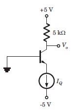
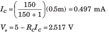
A device whose characteristics are very close to that of an ideal current source is- a)a BJT in CB mode
- b)a gas diode
- c)a triode
- d)a BJT in CE mode
Correct answer is option 'A'. Can you explain this answer?
A device whose characteristics are very close to that of an ideal current source is
a)
a BJT in CB mode
b)
a gas diode
c)
a triode
d)
a BJT in CE mode
| | Raj Singh answered |
The output characteristic of a CB transistor configuration is shown in figure below.
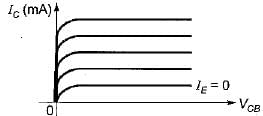
It is clear that for a constant value of IE, IC is independent of VCB and the curves are parallel to the axis of VCB.
Hence, a CB transistor acts as an ideal current source.
It is clear that for a constant value of IE, IC is independent of VCB and the curves are parallel to the axis of VCB.
Hence, a CB transistor acts as an ideal current source.
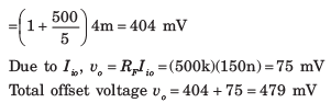
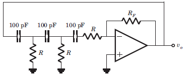
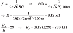
It is desired to reduce total harmonic of amplifier from 8% to 1% by use of 10% negative feedback. If the gain of the amplifier with original distortion and with reduced distortion is A1 and A2 then, A1 + A2 = −−−−−−
Correct answer is between '78.70,78.80'. Can you explain this answer?
It is desired to reduce total harmonic of amplifier from 8% to 1% by use of 10% negative feedback. If the gain of the amplifier with original distortion and with reduced distortion is A1 and A2 then, A1 + A2 = −−−−−−
| | Snehal Rane answered |
To solve this problem, we can use the formula for the reduction in distortion due to negative feedback:
Rd = 1 - (1 + β) * Hd
Where Rd is the reduction in distortion, β is the feedback factor, and Hd is the distortion without feedback.
Given that the reduction in distortion is desired to be from 8% to 1%, we can calculate the initial distortion without feedback (Hd) as:
Hd = 8% = 0.08
And the desired distortion with feedback (Hd') as:
Hd' = 1% = 0.01
We are also given that the feedback factor (β) is 10%.
Using the formula, we can calculate the reduction in distortion (Rd) as:
Rd = 1 - (1 + 0.1) * 0.08
= 1 - 1.08 * 0.08
= 1 - 0.0864
= 0.9136
Next, we can calculate the gain of the amplifier with reduced distortion (A2) using the formula:
A2 = A1 / (1 + β * A1 * Rd)
Where A1 is the gain of the amplifier with original distortion.
Since we want to find the relationship between A1 and A2, we can rearrange the formula to:
A2 = A1 / (1 + β * A1 * Rd)
A2 * (1 + β * A1 * Rd) = A1
A2 + β * A1 * Rd * A2 = A1
A2 - A1 = - β * A1 * Rd * A2
(A2 - A1) / (A1 * A2) = - β * Rd
(A2 - A1) / (A1 * A2 * Rd) = - β
Therefore, A1 * A2 = -(A2 - A1) / (β * Rd)
Substituting the values we have calculated:
A1 * A2 = -(A2 - A1) / (0.1 * 0.9136)
= -(A2 - A1) / 0.09136
The current gain of a common-emitter amplifier _____ as the load resistance is increased.- a)increases
- b)decreases
- c)in unchanged
- d)increase and then decreases
Correct answer is option 'B'. Can you explain this answer?
The current gain of a common-emitter amplifier _____ as the load resistance is increased.
a)
increases
b)
decreases
c)
in unchanged
d)
increase and then decreases
| | Prisha Iyer answered |
As the load resistance is increases, collector current reduces and hence current gain (β) is decreased.
An amplifier has a Open Loop voltage gain of –500. This gain is reduced to –100 when negative feedback is applied. The reverse transmission factor,β of this system is:-- a)– 0.025
- b)– 0.008
- c)0.1
- d)– 0.2
Correct answer is option 'B'. Can you explain this answer?
An amplifier has a Open Loop voltage gain of –500. This gain is reduced to –100 when negative feedback is applied. The reverse transmission factor,β of this system is:-
a)
– 0.025
b)
– 0.008
c)
0.1
d)
– 0.2
| | Pooja Patel answered |
Concept:
The gain of a feedback system is given by:

A = Open Loop gain
Af = Closed Loop Gain
β = Feedback/Transmission factor
Calculation:
Given Af = -100 and A = -500
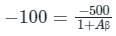
1 + Aβ = 5
Aβ = 4
β = 4 / -500 = -0.008
Primary trigger for oscillation is obtained from ___________- a)DC voltage
- b)Noise voltage
- c)External trigger voltage
- d)No trigger is required
Correct answer is option 'B'. Can you explain this answer?
Primary trigger for oscillation is obtained from ___________
a)
DC voltage
b)
Noise voltage
c)
External trigger voltage
d)
No trigger is required
| | Pooja Patel answered |
The primary trigger for oscillation is obtained from noise voltage.
When an electric field is applied across a semiconductor, free electrons in it will accelerate due to the applied field, and gain energy. This energy can be lost as heat when the electrons- a)recombine with holes
- b)collide with atoms in the crystal
- c)radiate energy while being accelerated
- d)collide with other electrons
Correct answer is option 'B'. Can you explain this answer?
When an electric field is applied across a semiconductor, free electrons in it will accelerate due to the applied field, and gain energy. This energy can be lost as heat when the electrons
a)
recombine with holes
b)
collide with atoms in the crystal
c)
radiate energy while being accelerated
d)
collide with other electrons
| | Nikhil Iyer answered |
Explanation:
When an electric field is applied across a semiconductor, the free electrons in the material experience a force due to the field. This force causes the electrons to accelerate and gain kinetic energy. However, this energy gained by the electrons is not permanently retained. Instead, it is lost as heat through collisions with atoms in the crystal lattice of the semiconductor material.
Collisions with Atoms in the Crystal:
- When the accelerated electrons collide with atoms in the crystal lattice, they transfer some of their kinetic energy to these atoms.
- These collisions cause the atoms to vibrate, increasing their thermal energy and consequently increasing the temperature of the material.
- This process is known as electron-phonon scattering, where phonons represent the lattice vibrations.
Reason for Choosing Option 'B':
- The other options listed (recombination with holes, radiation while being accelerated, and collision with other electrons) do not play a significant role in the loss of energy as heat in a semiconductor under an applied electric field.
- Recombination with holes refers to the combination of a free electron with an empty state (hole) in the valence band, resulting in the release of energy as light or heat. However, this process is not directly related to the loss of energy by accelerated electrons in an electric field.
- Radiation while being accelerated is more relevant in the context of charged particles moving close to the speed of light or in high-energy physics. In the case of electrons in a semiconductor under a typical electric field, the energy lost through radiation is negligible.
- Collisions with other electrons can lead to scattering and resistance in the material but do not directly result in the loss of energy as heat.
Conclusion:
When an electric field is applied across a semiconductor, the kinetic energy gained by the free electrons is lost primarily as heat through collisions with atoms in the crystal lattice. These collisions transfer energy to the lattice, increasing its thermal energy and causing the material to heat up. This phenomenon is an essential aspect of understanding the behavior of semiconductors under electric fields.

A properly biased JFET will act as a- a)current controlled current source
- b)voltage controlled voltage source
- c)voltage controlled current source
- d)current controlled voltage source
Correct answer is option 'C'. Can you explain this answer?
A properly biased JFET will act as a
a)
current controlled current source
b)
voltage controlled voltage source
c)
voltage controlled current source
d)
current controlled voltage source
| | Harshad Singh answered |
Due to high input impedance of JFET, it acts as a voltage controlled current source i.e. IG = 0 A.
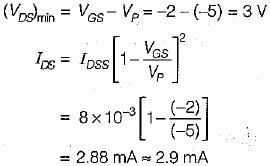
An N-channe! JFET has IDSS = 8 mA and Vp = -5 V. The minimum values of VDS for pinch- off region and the drain current IDS for VGS= - 2V in the pinch-off region are respectively.- a)2 V and 1.8 mA
- b)3 V and 2.9 mA
- c)2 V and 2.9 mA
- d)3 V and 1.8 mA
Correct answer is option 'B'. Can you explain this answer?
An N-channe! JFET has IDSS = 8 mA and Vp = -5 V. The minimum values of VDS for pinch- off region and the drain current IDS for VGS= - 2V in the pinch-off region are respectively.
a)
2 V and 1.8 mA
b)
3 V and 2.9 mA
c)
2 V and 2.9 mA
d)
3 V and 1.8 mA
| | Avik Iyer answered |
The minimum value of VDS for pinch-off to occur for VGS = -2V is
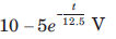
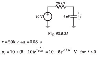
The circuit shown in fig. is at steady state before the switch opens at t = 0. The vc(t) for t > 0 is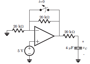
- a)
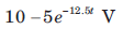
- b)
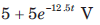
- c)
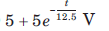
- d)
Correct answer is option 'A'. Can you explain this answer?
The circuit shown in fig. is at steady state before the switch opens at t = 0. The vc(t) for t > 0 is
a)
b)
c)
d)
| | Anjana Khatri answered |
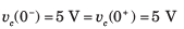
For t > 0 the equivalent circuit is shown in fig.
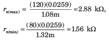
The nominal quiescent collector current of a transistor is 1.2 mA. If the range of β for this transistor is 80 ≤ β ≤ 120 and if the quiescent collector current changes by +-10 percent, the range in value for rπ is- a)1.73 kΩ < rπ < 2.59 kΩ
- b)1.93 kΩ < rπ < 2.59 kΩ
- c)1.73 kΩ < rπ < 2.59 kΩ
- d)1.56 kΩ < rπ < 2.88 kΩ
Correct answer is option 'D'. Can you explain this answer?
The nominal quiescent collector current of a transistor is 1.2 mA. If the range of β for this transistor is 80 ≤ β ≤ 120 and if the quiescent collector current changes by +-10 percent, the range in value for rπ is
a)
1.73 kΩ < rπ < 2.59 kΩ
b)
1.93 kΩ < rπ < 2.59 kΩ
c)
1.73 kΩ < rπ < 2.59 kΩ
d)
1.56 kΩ < rπ < 2.88 kΩ
 | Navya Sarkar answered |

Chapter doubts & questions for Analog Electronics - Topicwise Question Bank for Electrical Engineering 2026 is part of Electrical Engineering (EE) exam preparation. The chapters have been prepared according to the Electrical Engineering (EE) exam syllabus. The Chapter doubts & questions, notes, tests & MCQs are made for Electrical Engineering (EE) 2026 Exam. Find important definitions, questions, notes, meanings, examples, exercises, MCQs and online tests here.
Chapter doubts & questions of Analog Electronics - Topicwise Question Bank for Electrical Engineering in English & Hindi are available as part of Electrical Engineering (EE) exam. Download more important topics, notes, lectures and mock test series for Electrical Engineering (EE) Exam by signing up for free.