


All Exams >
NEET >
NEET Past Year Papers >
All Questions
All questions of Semiconductor Electronics for NEET Exam


The device that can act as a complete electroniccircuit is [2010]- a)junction diode
- b)integrated circuit
- c)junction transistor
- d)zener diode
Correct answer is option 'B'. Can you explain this answer?
The device that can act as a complete electroniccircuit is [2010]
a)
junction diode
b)
integrated circuit
c)
junction transistor
d)
zener diode

|
Rajeev Sharma answered |
Integrated circuit can act as a complete
electronic circuit.
electronic circuit.

Which one of the following bonds produces asolid that reflects light in the visible region andwhose electrical conductivity decreases withtemperature and has high melting point? [2010]- a)metallic bonding
- b)van der Waal's bonding
- c)ionic bonding
- d)covalent bonding
Correct answer is option 'A'. Can you explain this answer?
Which one of the following bonds produces asolid that reflects light in the visible region andwhose electrical conductivity decreases withtemperature and has high melting point? [2010]
a)
metallic bonding
b)
van der Waal's bonding
c)
ionic bonding
d)
covalent bonding

|
Naveen Menon answered |
For a metal, conductivity decreases with
increase in temperature.
Also, metal has high melting point.
increase in temperature.
Also, metal has high melting point.


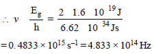
A p-n photodiode is made of a material with aband gap of 2.0 eV. The minimum frequency ofthe radiation that can be absorbed by the materialis nearly [2008]- a)10 × 1014 Hz
- b)5 ×10¹⁴ Hz
- c)1 × 10¹⁴ Hz
- d)20 × 1014 Hz
Correct answer is option 'B'. Can you explain this answer?
A p-n photodiode is made of a material with aband gap of 2.0 eV. The minimum frequency ofthe radiation that can be absorbed by the materialis nearly [2008]
a)
10 × 1014 Hz
b)
5 ×10¹⁴ Hz
c)
1 × 10¹⁴ Hz
d)
20 × 1014 Hz

|
Swara Desai answered |
Eg = 2.0 eV = 2 × 1.6 × 10–19 J
Eg = hv
Eg = hv
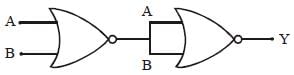
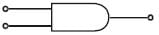
Symbolic representation of four logic gate are shown as [2011]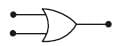
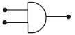
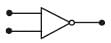
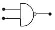 Pick out which ones are for AND, NAND and NOT gates, respectively
- a)(ii), (iii) and (iv)
- b)(iii), (ii) and (i)
- c)(iii), (iii) and (iv)
- d)(ii), (iv) and (iii)
Correct answer is option 'D'. Can you explain this answer?
Symbolic representation of four logic gate are shown as [2011]
Pick out which ones are for AND, NAND and NOT gates, respectively
a)
(ii), (iii) and (iv)
b)
(iii), (ii) and (i)
c)
(iii), (iii) and (iv)
d)
(ii), (iv) and (iii)
|
|
Ayaan Madhukar answered |
Simple bro...
Correct answer is option (D)...
Correct answer is option (D)...
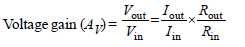
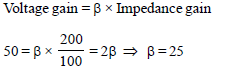
The input resistance of a silicon transistor is100 W. Base current is changed by 40 μA whichresults in a change in collector current by 2 mA.This transistor is used as a common emitteramplifier with a load resistance of 4 KΩ. Thevoltage gain of the amplifier is : [2012M]- a)2000
- b)3000
- c)4000
- d)1000
Correct answer is option 'A'. Can you explain this answer?
The input resistance of a silicon transistor is100 W. Base current is changed by 40 μA whichresults in a change in collector current by 2 mA.This transistor is used as a common emitteramplifier with a load resistance of 4 KΩ. Thevoltage gain of the amplifier is : [2012M]
a)
2000
b)
3000
c)
4000
d)
1000

|
Prasenjit Pillai answered |
The voltage gain of an amplifier with 9% negativefeedback is 10. The voltage gain withoutfeedback will be [2008]- a)90
- b)10
- c)1.25
- d)100
Correct answer is option 'D'. Can you explain this answer?
The voltage gain of an amplifier with 9% negativefeedback is 10. The voltage gain withoutfeedback will be [2008]
a)
90
b)
10
c)
1.25
d)
100

|
Kajal Bose answered |
Negative feedback is applied to reduce the
output voltage of an amplifier. If there is no
negative feedback, the value of output
voltage could be very high. In the options
given, the maximum value of voltage gain is
100. Hence it is the correct option.
output voltage of an amplifier. If there is no
negative feedback, the value of output
voltage could be very high. In the options
given, the maximum value of voltage gain is
100. Hence it is the correct option.
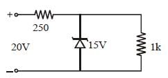
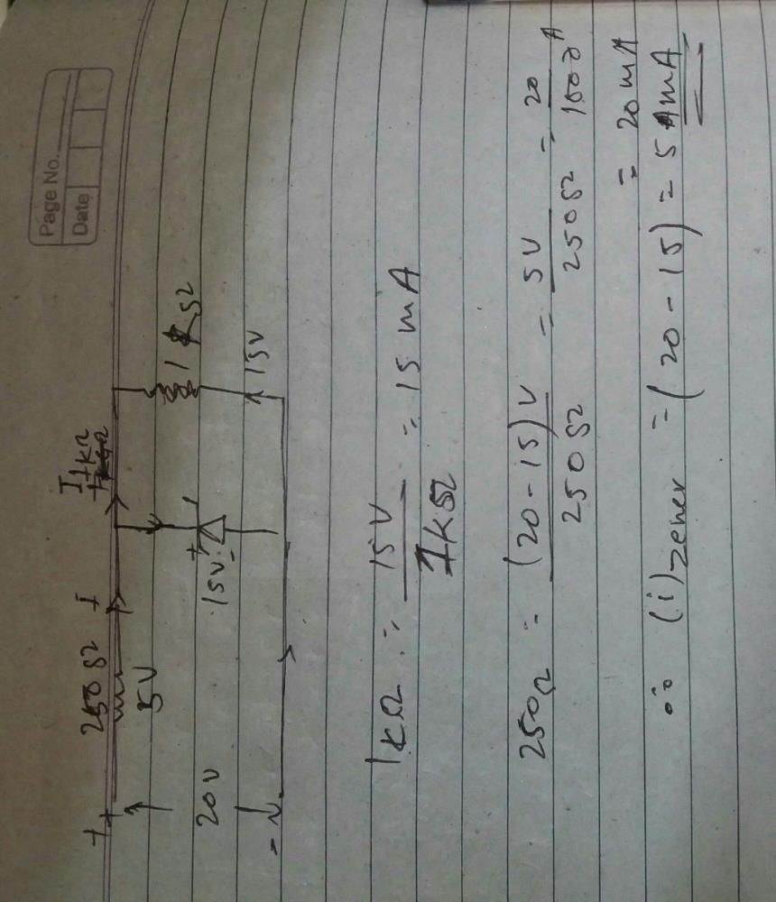
Zener diode is used for [2005]- a)amplification
- b)rectification
- c)stabilisation
- d)producing oscillations in an oscillator
Correct answer is option 'C'. Can you explain this answer?
Zener diode is used for [2005]
a)
amplification
b)
rectification
c)
stabilisation
d)
producing oscillations in an oscillator

|
Arya Khanna answered |
At a certain reverse bias voltage, zener diode
allows current to flow through it and hence
maintains the voltage supplied to any load
Hence, it is used for stabilisation.
allows current to flow through it and hence
maintains the voltage supplied to any load
Hence, it is used for stabilisation.
Choose the only false statement from thefollowing [2005]- a)In conductors, the valence and conductionbands may overlap
- b)Substances with energy gap of the order of10 eV are insulators
- c)The resistivity of a semiconductorincreases with increase in temperature
- d)The conductivity of a semiconductorincreases with increase in temperature
Correct answer is option 'C'. Can you explain this answer?
Choose the only false statement from thefollowing [2005]
a)
In conductors, the valence and conductionbands may overlap
b)
Substances with energy gap of the order of10 eV are insulators
c)
The resistivity of a semiconductorincreases with increase in temperature
d)
The conductivity of a semiconductorincreases with increase in temperature

|
Devansh Mehra answered |
(a) is true as in case of conductors either the
conduction & valence band overlap or
conduction band is partially filled.
(b) is true as insulators have energy gap of
the order of 5 to 10 eV.
(c) is false as resistivity (opposite of
conductivity) decreases with increase in
temperature.
(d) is true as with increase in temperature
more and more electrons jump to the
conduction band. So, conductivity increases.
Carbon, silicon and germanium atoms have fourvalence electrons each. Their valence andconduction bands are separated by energy bandgaps represented by (Eg)C, (Eg)Si and (Eg)Gerespectively. Which one of the followingrelationships is true in their case? [2005]- a)(Eg)C > (Eg)Si
- b)(Eg)C < (Eg)Si
- c)(Eg)C= (Eg)Si
- d)(Eg)C < (Eg)Ge
Correct answer is option 'A'. Can you explain this answer?
Carbon, silicon and germanium atoms have fourvalence electrons each. Their valence andconduction bands are separated by energy bandgaps represented by (Eg)C, (Eg)Si and (Eg)Gerespectively. Which one of the followingrelationships is true in their case? [2005]
a)
(Eg)C > (Eg)Si
b)
(Eg)C < (Eg)Si
c)
(Eg)C= (Eg)Si
d)
(Eg)C < (Eg)Ge

|
Sonal Kulkarni answered |
Due to strong electronegativity of carbon
Application of a forward bias to a p–n junction [2005]- a)widens the depletion zone
- b)increases the potential difference acrossthe depletion zone
- c)increases the number of donors on the nside
- d)increases the electric field in the depletionzone
Correct answer is option 'C'. Can you explain this answer?
Application of a forward bias to a p–n junction [2005]
a)
widens the depletion zone
b)
increases the potential difference acrossthe depletion zone
c)
increases the number of donors on the nside
d)
increases the electric field in the depletionzone

|
Mrinalini Bajaj answered |

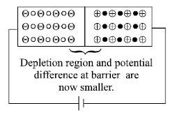
Number of donor s is more because
electrons from –ve terminal of the cell
pushes (enters) the n side and decreases
the number of uncompensated pentavalent
ion due to which potential barrier is
reduced. The neutralised pentavalent atom
are again in position to donate electrons.
electrons from –ve terminal of the cell
pushes (enters) the n side and decreases
the number of uncompensated pentavalent
ion due to which potential barrier is
reduced. The neutralised pentavalent atom
are again in position to donate electrons.
In a p-n junction photocell, the value of thephoto-electromotive force produced bymonochromatic light is proportional to [2004]- a)the voltage applied at the p-n junction
- b)the barrier voltage at the p-n junction
- c)the intensity of the light falling on the cell
- d)the frequency of the light falling on the cell
Correct answer is option 'C'. Can you explain this answer?
In a p-n junction photocell, the value of thephoto-electromotive force produced bymonochromatic light is proportional to [2004]
a)
the voltage applied at the p-n junction
b)
the barrier voltage at the p-n junction
c)
the intensity of the light falling on the cell
d)
the frequency of the light falling on the cell
|
|
Swara Desai answered |
Electromotive force depends upon intensity
of light falling, it does not depend on
frequency of barrier voltage
of light falling, it does not depend on
frequency of barrier voltage
In a CE transistor amplifier, the audio signalvoltage across the collector resistance of 2kΩ is 2V. If the base resistance is 1kΩ and thecurrent amplification of the transistor is 100, theinput signal voltage is : [2012]- a)0.1 V
- b)1.0 V
- c)1 mV
- d)10 mV
Correct answer is option 'D'. Can you explain this answer?
In a CE transistor amplifier, the audio signalvoltage across the collector resistance of 2kΩ is 2V. If the base resistance is 1kΩ and thecurrent amplification of the transistor is 100, theinput signal voltage is : [2012]
a)
0.1 V
b)
1.0 V
c)
1 mV
d)
10 mV

|
Ishaan Menon answered |
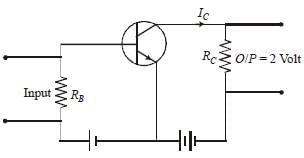
The output voltage, across the load RC
V0 = IC RC = 2
The collector current (IC)
V0 = IC RC = 2
The collector current (IC)
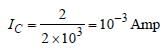
Current gain (β)
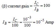
Input voltage (Vi)
Vi = RB IB = 1 × 10, × 10–5 = 10–2 Volt
Vi = 10 mV
Vi = RB IB = 1 × 10, × 10–5 = 10–2 Volt
Vi = 10 mV
Reverse bias applied to a junction diode [2003]- a)increases the minority carrier current
- b)lowers the potential barrier
- c)raises the potential barrier
- d)increases the majority carrier current
Correct answer is option 'C'. Can you explain this answer?
Reverse bias applied to a junction diode [2003]
a)
increases the minority carrier current
b)
lowers the potential barrier
c)
raises the potential barrier
d)
increases the majority carrier current

|
Pallabi Reddy answered |
In reverse biasing, the conduction across the
p-n junction does not take place due to
majority carriers but takes place due to
minority carriers if the voltage of external
battery is large. The size of the depletion
region increases thereby increasing the
potential barrier.
p-n junction does not take place due to
majority carriers but takes place due to
minority carriers if the voltage of external
battery is large. The size of the depletion
region increases thereby increasing the
potential barrier.
In the following figure, the diodes which are forward biased, are [2011M]

- a)(C) only
- b)(C) and (A)
- c)(B) and (D)
- d)(A), (B) and (D)
Correct answer is option 'B'. Can you explain this answer?
In the following figure, the diodes which are forward biased, are [2011M]
a)
(C) only
b)
(C) and (A)
c)
(B) and (D)
d)
(A), (B) and (D)
|
|
Saurabh Kumar answered |
High potential ( p_diode ) to low potential (n-diode ) concept
option b.
For transistor action :
(1) Base, emitter and collector regions should have similar size and doping concentrations.
(2) The base region must be very thin and lightly doped.
(3) The eimtter-base junction is forward biased and base-collector junction is reverse based.
(4) Both the emitter-base junction as well as the base-collector junction are forward biased.- a)(3), (4)
- b)(4), (1)
- c)(1), (2)
- d)(2), (3)
Correct answer is option 'D'. Can you explain this answer?
For transistor action :
(1) Base, emitter and collector regions should have similar size and doping concentrations.
(2) The base region must be very thin and lightly doped.
(3) The eimtter-base junction is forward biased and base-collector junction is reverse based.
(4) Both the emitter-base junction as well as the base-collector junction are forward biased.
a)
(3), (4)
b)
(4), (1)
c)
(1), (2)
d)
(2), (3)

|
Kunal Rane answered |
For transistor action, the base region must
be very thin and lightly doped. Also, the
emitter-base junction is forward biased and
base-collector junction is reverse biased
be very thin and lightly doped. Also, the
emitter-base junction is forward biased and
base-collector junction is reverse biased
In forward biasing of the p–n junction [2011]- a)the positive terminal of the battery isconnected to p–side and the depletionregion becomes thick
- b)the positive terminal of the battery isconnected to n–side and the depletionregion becomes thin
- c)the positive terminal of the battery isconnected to n–side and the depletionregion becomes thick
- d)the positive terminal of the battery isconnected to p–side and the depletionregion becomes thin
Correct answer is option 'D'. Can you explain this answer?
In forward biasing of the p–n junction [2011]
a)
the positive terminal of the battery isconnected to p–side and the depletionregion becomes thick
b)
the positive terminal of the battery isconnected to n–side and the depletionregion becomes thin
c)
the positive terminal of the battery isconnected to n–side and the depletionregion becomes thick
d)
the positive terminal of the battery isconnected to p–side and the depletionregion becomes thin

|
Ayush Chavan answered |
In forward biasing of the p-n junction, the
positive terminal of the battery is connected
to p-side and the negative terminal of the
battery is connected to n-side. The depletion
region becomes thin.
positive terminal of the battery is connected
to p-side and the negative terminal of the
battery is connected to n-side. The depletion
region becomes thin.
Pure Si at 500K has equal number ofelectron (ne) and hole (nh) concentrations of1.5 × 1016 m–3. Doping by indium increases nhto 4.5 × 10²² m–3. The doped semiconductor isof [2011M]- a)n–type with electron concentrationne = 5 × 10²² m–3
- b)p–type with electron concentrationne = 2.5 ×10¹⁰ m–3
- c)n–type with electron concentrationne = 2.5 × 10²³ m–3
- d)p–type having electron concentrationne = 5 × 10⁹ m–3
Correct answer is option 'D'. Can you explain this answer?
Pure Si at 500K has equal number ofelectron (ne) and hole (nh) concentrations of1.5 × 1016 m–3. Doping by indium increases nhto 4.5 × 10²² m–3. The doped semiconductor isof [2011M]
a)
n–type with electron concentrationne = 5 × 10²² m–3
b)
p–type with electron concentrationne = 2.5 ×10¹⁰ m–3
c)
n–type with electron concentrationne = 2.5 × 10²³ m–3
d)
p–type having electron concentrationne = 5 × 10⁹ m–3

|
Deepak Joshi answered |
or ne = 5 × 10⁹
Given nh = 4.5 × 10²²
⇒nh >> ne
∴ Semiconductor is p-type and
ne = 5 × 10⁹ m–3.
Given nh = 4.5 × 10²²
⇒nh >> ne
∴ Semiconductor is p-type and
ne = 5 × 10⁹ m–3.
In a common emitter (CE) amplifier having a voltage gain G, the transistor used has transconductance 0.03 mho and current gain 25. If the above transistor is replaced with another one with transconductance 0.02 mho and current gain 20, the voltage gain will be [NEET 2013] - a)1.5 G
- b)1/3 G
- c)5/4 G
- d)2/3 G
Correct answer is option 'D'. Can you explain this answer?
In a common emitter (CE) amplifier having a voltage gain G, the transistor used has transconductance 0.03 mho and current gain 25. If the above transistor is replaced with another one with transconductance 0.02 mho and current gain 20, the voltage gain will be [NEET 2013]
a)
1.5 G
b)
1/3 G
c)
5/4 G
d)
2/3 G
|
|
Isha Rane answered |
Given:
Transconductance of 1st transistor (gm1) = 0.03 mho
Current gain of 1st transistor (β1) = 25
Voltage gain of Common Emitter amplifier = G
To Find:
Voltage gain of Common Emitter amplifier when the transistor is replaced with another one with gm2 = 0.02 mho and β2 = 20
Solution:
We know that the voltage gain of a common emitter amplifier is given by the formula:
G = -gm * R_c * β
Where gm is the transconductance of the transistor, Rc is the collector resistance and β is the current gain.
Let's assume that the collector resistance remains the same in both cases. Therefore, we can write:
G1 = -gm1 * Rc * β1
G2 = -gm2 * Rc * β2
Dividing G2 by G1, we get:
G2/G1 = (-gm2 * Rc * β2) / (-gm1 * Rc * β1)
Simplifying the above equation, we get:
G2/G1 = (gm1/gm2) * (β2/β1)
Substituting the given values, we get:
G2/G1 = (0.03/0.02) * (20/25) = 0.9
Therefore, the voltage gain of the common emitter amplifier when the transistor is replaced with another one with gm2 = 0.02 mho and β2 = 20 is:
G2 = G1 * (G2/G1) = G * 0.9
G2 = 0.9G
Hence, the correct option is (d) 2/3 G.
C and Si both have same lattice structure, having 4 bonding electrons in each. However, C isinsulator whereas Si is intrinsic semiconductor.This is because : [2012]- a)In case of C the valence band is notcompletely filled at absolute zerotemperature.
- b)In case of C the conduction band is partlyfilled even at absolute zero temperature.
- c)The four bonding electrons in the case of Clie in the second orbit, whereas in the caseof Si they lie in the third.
- d)The four bonding electrons in the case of Clie in the third orbit, whereas for Si they liein the fourth orbit.
Correct answer is option 'C'. Can you explain this answer?
C and Si both have same lattice structure, having 4 bonding electrons in each. However, C isinsulator whereas Si is intrinsic semiconductor.This is because : [2012]
a)
In case of C the valence band is notcompletely filled at absolute zerotemperature.
b)
In case of C the conduction band is partlyfilled even at absolute zero temperature.
c)
The four bonding electrons in the case of Clie in the second orbit, whereas in the caseof Si they lie in the third.
d)
The four bonding electrons in the case of Clie in the third orbit, whereas for Si they liein the fourth orbit.
|
|
Subhankar Choudhary answered |
Explanation:
C and Si have the same lattice structure, but their electrical properties are different. The reason for this difference lies in the electronic configuration of the two elements.
Valence electrons
Both C and Si have 4 valence electrons, which are involved in bonding. The electronic configuration of C is 1s2 2s2 2p2, while that of Si is 1s2 2s2 2p6 3s2 3p2. This means that the valence electrons of C lie in the second orbit, whereas those of Si lie in the third orbit.
Bonding
The valence electrons of C and Si are involved in covalent bonding, which means that they share electrons with their neighboring atoms. In the case of C, each atom forms 4 covalent bonds, resulting in a very stable structure. However, this stable structure also means that the valence band is not completely filled at absolute zero temperature. Therefore, C is an insulator.
Intrinsic semiconductor
On the other hand, Si is an intrinsic semiconductor because its valence band is completely filled at absolute zero temperature, but there is a small energy gap between the valence band and the conduction band. This energy gap is small enough that thermal energy can cause electrons to jump from the valence band to the conduction band, allowing the material to conduct electricity. This property of semiconductors is utilized in many electronic devices.
Conclusion
In summary, the difference in electronic configuration between C and Si leads to differences in their electrical properties. While C is an insulator due to the incomplete filling of its valence band, Si is an intrinsic semiconductor due to the small energy gap between its valence and conduction bands.
For a cubic crystal structure which one of thefollowing relations indicating the cellcharacteristics is correct? [2007]- a)a ≠ b ≠ c and α = β = γ = 90°
- b)a = b = c and α ≠ β ≠ γ = 90°
- c)a = b = c and α = β = γ = 90°
- d)a ≠ b ≠ c and α ≠ β and γ ≠ 90°
Correct answer is option 'C'. Can you explain this answer?
For a cubic crystal structure which one of thefollowing relations indicating the cellcharacteristics is correct? [2007]
a)
a ≠ b ≠ c and α = β = γ = 90°
b)
a = b = c and α ≠ β ≠ γ = 90°
c)
a = b = c and α = β = γ = 90°
d)
a ≠ b ≠ c and α ≠ β and γ ≠ 90°
|
|
Sonal Kulkarni answered |
For a cubic crystal,
a = b = c and α = β = γ = 90°
a = b = c and α = β = γ = 90°
In a n-type semiconductor, which of the followingstatement is true? [NEET 2013]- a)Electrons are minority carriers andpentavalent atoms are dopants.
- b)Holes are minority carriers and pentavalentatoms are dopants.
- c)Holes are majority carriers and trivalentatoms are dopants.
- d)Electrons are majority carriers and trivalentatoms are dopants.
Correct answer is option 'B'. Can you explain this answer?
In a n-type semiconductor, which of the followingstatement is true? [NEET 2013]
a)
Electrons are minority carriers andpentavalent atoms are dopants.
b)
Holes are minority carriers and pentavalentatoms are dopants.
c)
Holes are majority carriers and trivalentatoms are dopants.
d)
Electrons are majority carriers and trivalentatoms are dopants.
|
|
Ayush Chavan answered |
In a n-type semiconductor holes are
minority carriers and pentavalent atoms
are dopants.
minority carriers and pentavalent atoms
are dopants.
If a small amount of antimony is added togermanium crystal [2011]- a)it becomes a p–type semiconductor
- b)the antimony becomes an acceptor atom
- c)there will be more free electrons than holesin the semiconductor
- d)its resistance is increased
Correct answer is option 'C'. Can you explain this answer?
If a small amount of antimony is added togermanium crystal [2011]
a)
it becomes a p–type semiconductor
b)
the antimony becomes an acceptor atom
c)
there will be more free electrons than holesin the semiconductor
d)
its resistance is increased

|
Rohan Unni answered |
When small amount of antimony
(pentavalent) is added to germanium crystal
then crystal becomes n-type semi conductor.
Therefore, there will be more free electrons
than holes in the semiconductor.
(pentavalent) is added to germanium crystal
then crystal becomes n-type semi conductor.
Therefore, there will be more free electrons
than holes in the semiconductor.
Transfer characteristics [output voltage (V0) vs input voltage (V1)] for a base biased transistor in CE configuration is as shown in the figure. For using transistor as a switch, it is used : [2012]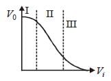
- a)in region III
- b)both in region (I) and (III)
- c)in region II
- d)in region (I)
Correct answer is option 'B'. Can you explain this answer?
Transfer characteristics [output voltage (V0) vs input voltage (V1)] for a base biased transistor in CE configuration is as shown in the figure. For using transistor as a switch, it is used : [2012]
a)
in region III
b)
both in region (I) and (III)
c)
in region II
d)
in region (I)
|
|
Kunal Rane answered |
I → ON
II → OFF
In IInd state it is used as a amplifier it is
active region
II → OFF
In IInd state it is used as a amplifier it is
active region
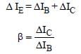
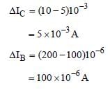
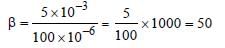
A transistor is operated in common emitterconfiguration at VC = 2V such that a change inthe base current from 100 μA to 300 μA producesa change in the collector current from 10mA to20 mA. The current gain is [2011]- a)50
- b)75
- c)100
- d)25
Correct answer is option 'A'. Can you explain this answer?
A transistor is operated in common emitterconfiguration at VC = 2V such that a change inthe base current from 100 μA to 300 μA producesa change in the collector current from 10mA to20 mA. The current gain is [2011]
a)
50
b)
75
c)
100
d)
25
|
|
Prasenjit Pillai answered |
The current gain
A transistor is operated in common-emitterconfiguration at Vc = 2 V such that a change inthe base current from 100 μA to 200 μA producesa change in the collector current from 5 mA to10 mA. The current gain is [2009]- a)100
- b)150
- c)50
- d)75
Correct answer is option 'C'. Can you explain this answer?
A transistor is operated in common-emitterconfiguration at Vc = 2 V such that a change inthe base current from 100 μA to 200 μA producesa change in the collector current from 5 mA to10 mA. The current gain is [2009]
a)
100
b)
150
c)
50
d)
75

|
Anu Bajaj answered |
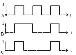
The following Figure shows a logic gate circuit with two inputs A and B and the output Y. The voltage waveforms of A, B and Y are given :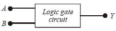
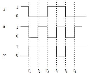 The logic gate is :
- a)NAND gate
- b)NOR gate
- c)OR gate
- d)AND gate
Correct answer is option 'A'. Can you explain this answer?
The following Figure shows a logic gate circuit with two inputs A and B and the output Y. The voltage waveforms of A, B and Y are given :
The logic gate is :
a)
NAND gate
b)
NOR gate
c)
OR gate
d)
AND gate

|
Aniket Chawla answered |
From the given waveforms, the truth table
is as follows.
is as follows.
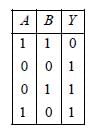
The above truth table is for NAND gate.
Therefore, the logic gate is NAND gate.
Therefore, the logic gate is NAND gate.
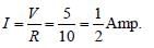
Two ideal diodes are connected to a battery as shown in the circuit. The current supplied by the battery is :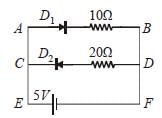
- a)0.75 A
- b)zero
- c)0.25 A
- d)0.5 A
Correct answer is option 'D'. Can you explain this answer?
Two ideal diodes are connected to a battery as shown in the circuit. The current supplied by the battery is :
a)
0.75 A
b)
zero
c)
0.25 A
d)
0.5 A
|
|
Aniket Chawla answered |
Here D1 is in forward bias and D2 is in
reverse bias so, D1 will conduct and D2 will
not conduct. Thus, no current will flow
through DC.
reverse bias so, D1 will conduct and D2 will
not conduct. Thus, no current will flow
through DC.
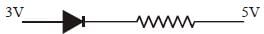
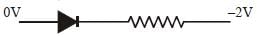
A forward biased diode is [2006]- a)
- b)
- c)
- d)
Correct answer is option 'C'. Can you explain this answer?
A forward biased diode is [2006]
a)
b)
c)
d)
|
|
Pallabi Reddy answered |
In forward biasing of a diode, the emitted
should be at a higher potential, Here, only in
option (c) emitter is at higher potential with
bias voltage 0V compared to the collector,
which is at –2V. So, it is reverse biased.
should be at a higher potential, Here, only in
option (c) emitter is at higher potential with
bias voltage 0V compared to the collector,
which is at –2V. So, it is reverse biased.
In the energy band diagram of a material shown below, the open circles and filled circles denote holes and electrons respectively. The material is [2007]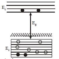
- a)an insulator
- b)a metal
- c)an n-type semiconductor
- d)a p-type semiconductor
Correct answer is option 'D'. Can you explain this answer?
In the energy band diagram of a material shown below, the open circles and filled circles denote holes and electrons respectively. The material is [2007]
a)
an insulator
b)
a metal
c)
an n-type semiconductor
d)
a p-type semiconductor

|
Pankaj Banerjee answered |
For a p-type semiconductor, the acceptor
energy level, as shown in the diagram, is
slightly above the top Ev of the valence band.
With very small supply of energy an electron
from the valence band can jump to the level
EA and ionise acceptor negatively.
energy level, as shown in the diagram, is
slightly above the top Ev of the valence band.
With very small supply of energy an electron
from the valence band can jump to the level
EA and ionise acceptor negatively.


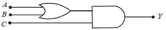
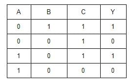
The following figure shows a logic gate circuit with two inputs A and B and the output C. The voltage waveforms of A, B and C are as shown below
 The logic circuit gate is [2006]
- a)NAND gate
- b)NOR gate
- c)OR gate
- d)AND gate
Correct answer is option 'D'. Can you explain this answer?
The following figure shows a logic gate circuit with two inputs A and B and the output C. The voltage waveforms of A, B and C are as shown below
The logic circuit gate is [2006]
a)
NAND gate
b)
NOR gate
c)
OR gate
d)
AND gate
|
|
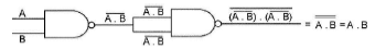
Pankaj Banerjee answered |
On the basis of given graph, following table
is possible.
is possible.
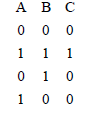
It is the truth table of AND gate.
A transistor is operated in common emitterconfiguration at constant collector voltage Vc =1.5V such that a change in the base current from100 μA to 150 μA produces a change in thecollector current from 5 mA to 10 mA. The currentgain (β) is [2006]- a)75
- b)100
- c)50
- d)67
Correct answer is option 'B'. Can you explain this answer?
A transistor is operated in common emitterconfiguration at constant collector voltage Vc =1.5V such that a change in the base current from100 μA to 150 μA produces a change in thecollector current from 5 mA to 10 mA. The currentgain (β) is [2006]
a)
75
b)
100
c)
50
d)
67

|
Muskaan Basak answered |
A p-n photodiode is fabricated from a semiconductor with a band gap of 2.5 eV. It candetect a signal of wavelength [2009]- a)4000 nm
- b)6000 nm
- c)4000 Å
- d)6000 Å
Correct answer is option 'C'. Can you explain this answer?
A p-n photodiode is fabricated from a semiconductor with a band gap of 2.5 eV. It candetect a signal of wavelength [2009]
a)
4000 nm
b)
6000 nm
c)
4000 Å
d)
6000 Å

|
Ruchi Chopra answered |

The wavelength detected by photodiode
should be less than λmax. Hence it can
detect a signal of wavelength 4000Å.
should be less than λmax. Hence it can
detect a signal of wavelength 4000Å.


The output of OR gate is 1 [2004]- a)if either input is zero
- b)if both inputs are zero
- c)if either or both inputs are 1
- d)only if both inputs are 1
Correct answer is option 'C'. Can you explain this answer?
The output of OR gate is 1 [2004]
a)
if either input is zero
b)
if both inputs are zero
c)
if either or both inputs are 1
d)
only if both inputs are 1

|
Arpita Tiwari answered |
Output will be one if A or B or both are one.
Y= A + B
Y= A + B
In semiconductors, at room temperature [2004]- a)the conduction band is completely empty
- b)the valence band is partially empty and theconduction band is partially filled
- c)the valence band is completely filled andthe conduction band is partially filled
- d)the valence band is completely filled
Correct answer is option 'C'. Can you explain this answer?
In semiconductors, at room temperature [2004]
a)
the conduction band is completely empty
b)
the valence band is partially empty and theconduction band is partially filled
c)
the valence band is completely filled andthe conduction band is partially filled
d)
the valence band is completely filled

|
Subhankar Datta answered |
In semiconductors, the conduction band is
empty and the valence band is completely
filled at 0 K. No electron from valence band
can cross over to conduction band at 0K.
But at room temperature some electrons in
the valence band jump over to the
conduction band due to the small forbidden
gap, i.e. 1 eV.
empty and the valence band is completely
filled at 0 K. No electron from valence band
can cross over to conduction band at 0K.
But at room temperature some electrons in
the valence band jump over to the
conduction band due to the small forbidden
gap, i.e. 1 eV.
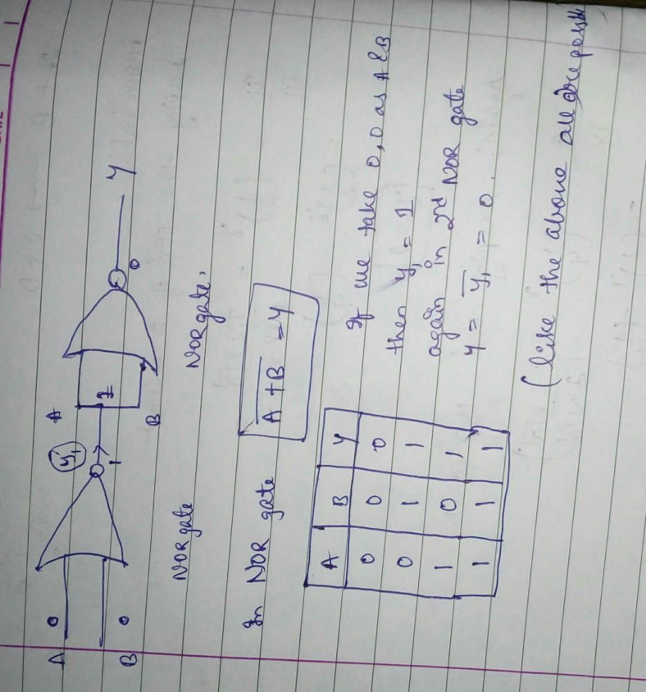
The circuit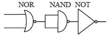 is equivalent to
- a)AND gate
- b)NAND gate
- c)NOR gate
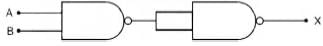
- d)OR gate
Correct answer is option 'C'. Can you explain this answer?
The circuit
is equivalent to
a)
AND gate
b)
NAND gate
c)
NOR gate
d)
OR gate
|
|
Subhankar Datta answered |
Let A and B be inputs and Y the output
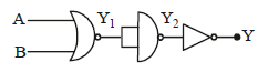
Then Y1 
Hence, the given circuit is equivalent to a
NOR gate.
NOR gate.

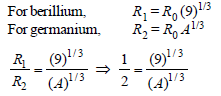
The radius of germanium (Ge) nuclide ismeasured to be twice the radius of 94Be . Thenumber of nucleons in Ge are [2006]- a)74
- b)75
- c)72
- d)73
Correct answer is option 'C'. Can you explain this answer?
The radius of germanium (Ge) nuclide ismeasured to be twice the radius of 94Be . Thenumber of nucleons in Ge are [2006]
a)
74
b)
75
c)
72
d)
73
|
|
Devansh Mehra answered |
We use the formula,
R = R0 A1/3
This represents relation between atomic mass
and radius of the nucleus.
R = R0 A1/3
This represents relation between atomic mass
and radius of the nucleus.
The number of beta particles emitted by aradioactive substance is twice the number ofalpha particles emitted by it. The resultingdaughter is an [2009]- a)isomer of parent
- b)isotone of parent
- c)isotope of parent
- d)isobar of parent
Correct answer is option 'C'. Can you explain this answer?
The number of beta particles emitted by aradioactive substance is twice the number ofalpha particles emitted by it. The resultingdaughter is an [2009]
a)
isomer of parent
b)
isotone of parent
c)
isotope of parent
d)
isobar of parent

|
Krish Saha answered |
Isotopes of an element have the same atomic
number but different mass number. A
radioactive substance when emits one alpha
particles its mass number reduces
by 4 and charge no. reduces by 2 and after
emission of two β-particles its charge no.
increase by 2 thus the charge no. i.e. atomic
number remains the same.
number but different mass number. A
radioactive substance when emits one alpha
particles
its mass number reducesby 4 and charge no. reduces by 2 and after
emission of two β-particles its charge no.
increase by 2 thus the charge no. i.e. atomic
number remains the same.
The figure shows a logic circuit with two inputs A and B and the output C. The voltage wave forms across A, B and C are as given. The logic circuit gate is : [2012]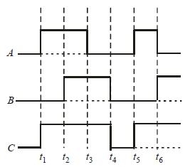
- a)OR gate
- b)NOR gate
- c)AND gate
- d)NAND gate
Correct answer is option 'A'. Can you explain this answer?
The figure shows a logic circuit with two inputs A and B and the output C. The voltage wave forms across A, B and C are as given. The logic circuit gate is : [2012]
a)
OR gate
b)
NOR gate
c)
AND gate
d)
NAND gate
|
|
Satyam answered |
A se the graph carefully
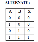
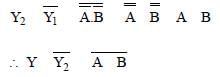
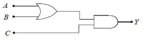
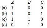
To get an output Y = 1 in the given circuit which of the following input will be correct:
[2012M]
- a)a
- b)b
- c)c
- d)d
Correct answer is option 'B'. Can you explain this answer?
To get an output Y = 1 in the given circuit which of the following input will be correct:
[2012M]
[2012M]
a)
a
b)
b
c)
c
d)
d
|
|
Deepak Joshi answered |
When A = 1, B = 0, C = 1 then Y = 1
y1 = 1 + 0 = 1
y = y1C = 1.1 = 1
y1 = 1 + 0 = 1
y = y1C = 1.1 = 1
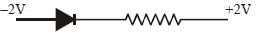
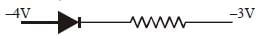
Of the diodes shown in following diagrams, which one is reverse biased ? [2004]- a)
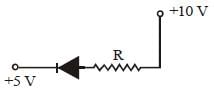
- b)
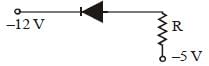
- c)
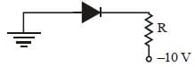
- d)
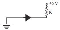
Correct answer is option 'D'. Can you explain this answer?
Of the diodes shown in following diagrams, which one is reverse biased ? [2004]
a)
b)
c)
d)

|
Arya Nair answered |
Positive terminal is at lower potential (0V)
and negative terminal is at higher potential
+5 V
and negative terminal is at higher potential
+5 V
The symbolic representation of four logic gates are given below : [2009]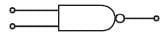
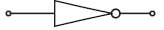
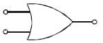 The logic symbols for OR, NOT and NAND gates are respectively:
- a)(iv), (i), (iii)
- b)(iv), (ii), (i)
- c)(i), (iii), (iv)
- d)(iii), (iv), (ii)
Correct answer is option 'B'. Can you explain this answer?
The symbolic representation of four logic gates are given below : [2009]
The logic symbols for OR, NOT and NAND gates are respectively:
a)
(iv), (i), (iii)
b)
(iv), (ii), (i)
c)
(i), (iii), (iv)
d)
(iii), (iv), (ii)
|
|
Muskaan Basak answered |
(iv), (ii), (i)
Option (iii) represents AND gate.
Chapter doubts & questions for Semiconductor Electronics - NEET Past Year Papers 2025 is part of NEET exam preparation. The chapters have been prepared according to the NEET exam syllabus. The Chapter doubts & questions, notes, tests & MCQs are made for NEET 2025 Exam. Find important definitions, questions, notes, meanings, examples, exercises, MCQs and online tests here.
Chapter doubts & questions of Semiconductor Electronics - NEET Past Year Papers in English & Hindi are available as part of NEET exam.
Download more important topics, notes, lectures and mock test series for NEET Exam by signing up for free.
NEET Past Year Papers
86 docs|146 tests
|
|
© EduRev
|
Education Revolution
|


|


Signup to see your scores
go up
within 7 days!
within 7 days!
Takes less than 10 seconds to signup