


All questions of Basic Electronics for Electrical Engineering (EE) Exam
Which of the following is a unipolar diode?- a)Zener diode
- b)Step recovery diode
- c)Schottky diode
- d)All of these
Correct answer is option 'C'. Can you explain this answer?
Which of the following is a unipolar diode?
a)
Zener diode
b)
Step recovery diode
c)
Schottky diode
d)
All of these

|
Engineers Adda answered |
In a unipolar device current is due to only one type of carriers (i.e. electrons or holes), while in bipolar device current is due to both holes and electrons.
Schottky diode or hot-carrier diode is a junction of n-type semiconductor and metal, in it electrons are sole carriers.

The depletion region of PN junction is consist of:- a)Atoms
- b)Passive component
- c)Mobile charges
- d)Immobile charge
Correct answer is option 'D'. Can you explain this answer?
The depletion region of PN junction is consist of:
a)
Atoms
b)
Passive component
c)
Mobile charges
d)
Immobile charge
|
|
Rhea Reddy answered |
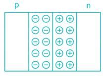
The holes from p-region cross the p-n Junction and recombine with electrons on the n-region. Similarly the electrons form n-region cross the junction & recombine with holes in p-region. Leaving immobile ions behind.
Thus the region near the junction is devoid of any mobile charge carriers, due to their recombination. Hence Depletion region of p-n Junction consists of immobile charges.
Which of the following is not possible BJT configuration?- a)Common base configuration
- b)Common emitter configuration
- c)Common current configuration
- d)Common collector configuration
Correct answer is option 'C'. Can you explain this answer?
Which of the following is not possible BJT configuration?
a)
Common base configuration
b)
Common emitter configuration
c)
Common current configuration
d)
Common collector configuration
|
|
Yash Patel answered |
The 3 configurations in BJT are
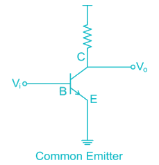
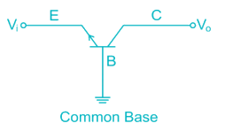
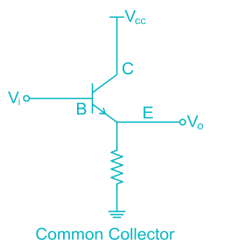
The term “Common” refers to the Common terminal through which input is given and from which output is withdrawn i.e. common terminal between input and output.
The term common current is logically incorrect and is not a BJT Configuration.
The phenomenon of thermal run away is associated with- a)Vacuum tubes
- b)Transistors
- c)Gas diode
- d)All of these
Correct answer is option 'B'. Can you explain this answer?
The phenomenon of thermal run away is associated with
a)
Vacuum tubes
b)
Transistors
c)
Gas diode
d)
All of these

|
Rishika Sen answered |
Thermal runaway is a situation in which increase in temperature changes the conditions in a way that further causes temperature to increase.
In BJTs the collector current dissipates lot of heat, this increase in temperature causes increased flow of minority carriers from collector to base, further increasing the collector current. This increase in collector current further raise temperature, thus thermal runaway occurs ending in burnout of BJT.
ICBO in a transistor can be reduced by reducing:- a)IB
- b)VCC
- c)IE
- d)Temperature
Correct answer is option 'D'. Can you explain this answer?
ICBO in a transistor can be reduced by reducing:
a)
IB
b)
VCC
c)
IE
d)
Temperature
|
|
Sanvi Kapoor answered |
ICBO is the reverse leakage current between collector and base while emitter is open it is given by ICBO=(1−α)IC−αIB. It is the reverse current in base collector junction, which is dependent on temperature at the junction and is reduced with decreasing current.
Of the three BJT configurations CB, CE and CC:- a)CB does not have miller effect hence higher bandwidth
- b)CC has smallest bandwidth
- c)CB exhibits reduction in bandwidth due to Miller effect
- d)CE exhibits increase in bandwidth due to Miller effect
Correct answer is option 'A'. Can you explain this answer?
Of the three BJT configurations CB, CE and CC:
a)
CB does not have miller effect hence higher bandwidth
b)
CC has smallest bandwidth
c)
CB exhibits reduction in bandwidth due to Miller effect
d)
CE exhibits increase in bandwidth due to Miller effect
|
|
Swati Shah answered |
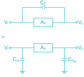
Av = gain of Amplifier
Miller Capacitance
CM = CC (1 + AV)
The increase in input capacitance decreases the upper cut off frequency
In case of CB configuration there is no miller capacitance between input and output & hence upper cut off frequency (fH) is high & higher Bandwidth
Fermi level is the measure of- a)Doping of electrons
- b)Probability of occupancy of electrons or holes
- c)Probability of occupancy of photons
- d)Probability of occupancy of wavelength
Correct answer is option 'B'. Can you explain this answer?
Fermi level is the measure of
a)
Doping of electrons
b)
Probability of occupancy of electrons or holes
c)
Probability of occupancy of photons
d)
Probability of occupancy of wavelength
|
|
Partho Saha answered |
From the definition of fermi level, the fermi level is energy state having probability ‘1/2’ of being occupied by an electron.
The cascade amplifier is a multistage configuration of:- a)CC – CB
- b)CE – CB
- c)CB – CC
- d)CE –CC
Correct answer is option 'B'. Can you explain this answer?
The cascade amplifier is a multistage configuration of:
a)
CC – CB
b)
CE – CB
c)
CB – CC
d)
CE –CC
|
|
Dhruv Datta answered |
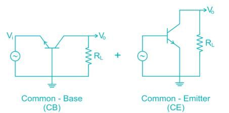
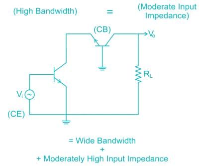
Hence cascade is CE – CB Configuration
DC bias is adjusted greater than its cut-off value so that the output current flow for less than half of the input voltage cycle, in:- a)Class A amplifier
- b)Class B amplifier
- c)Class C amplifier
- d)Class AB amplifier
Correct answer is option 'C'. Can you explain this answer?
DC bias is adjusted greater than its cut-off value so that the output current flow for less than half of the input voltage cycle, in:
a)
Class A amplifier
b)
Class B amplifier
c)
Class C amplifier
d)
Class AB amplifier
|
|
Rahul Chakraborty answered |
Understanding DC Bias in Amplifiers
DC biasing is crucial in amplifier design as it sets the operating point of the transistor. In the context of the question, we are particularly focused on Class C amplifiers.
Class C Amplifier Characteristics
- Class C amplifiers are designed for high-efficiency applications.
- They operate with a DC bias level greater than the cut-off value, which ensures that the output current flows for less than half of the input voltage cycle.
- This configuration results in a conduction angle of less than 180 degrees.
Key Features of Class C Operation
- Efficiency: Class C amplifiers can achieve efficiencies above 80% due to their short conduction time.
- Signal Distortion: Since they only conduct for a portion of the input cycle, Class C amplifiers often introduce significant distortion.
- Ideal for RF Applications: They are commonly used in radio frequency (RF) applications where high efficiency is paramount, such as in transmitters.
Comparison with Other Classes
- Class A: Conducts for the entire input cycle (360 degrees), making it less efficient.
- Class B: Conducts for half of the input cycle (180 degrees), providing better efficiency than Class A.
- Class AB: Operates between Class A and Class B, conducting slightly more than half the cycle, which improves linearity while maintaining efficiency.
Conclusion
In summary, the correct answer is Class C amplifier, as it is specifically designed to operate with a DC bias above its cut-off value, allowing current to flow for less than half of the input voltage cycle, making it ideal for high-efficiency applications.
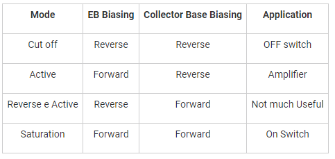
When a BJT is used as switch, its mode of operation switches between:- a)Cut-off and active regions
- b)Cut-off and saturation regions
- c)Active and saturation regions
- d)Different operating points in the active region
Correct answer is option 'B'. Can you explain this answer?
When a BJT is used as switch, its mode of operation switches between:
a)
Cut-off and active regions
b)
Cut-off and saturation regions
c)
Active and saturation regions
d)
Different operating points in the active region
|
|
Megha Datta answered |
Different modes of BJT operations
For switching Application BJT is operated in cut off (off switch) and saturation (on switch)
Which of the following diode is used for voltage stabilization?- a)P – N junction
- b)Zener
- c)Tunnel
- d)PIN
Correct answer is option 'B'. Can you explain this answer?
Which of the following diode is used for voltage stabilization?
a)
P – N junction
b)
Zener
c)
Tunnel
d)
PIN
|
|
Bhavana Reddy answered |
The I - V characteristic of Zener diode is shown
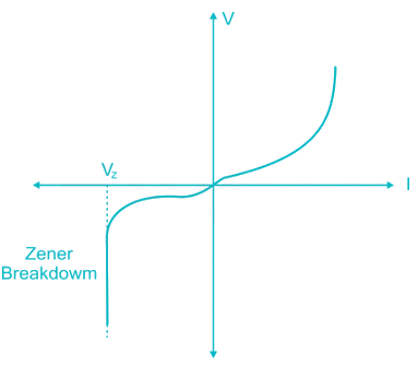
When Zener diode is reversed Biased the voltage across it is constant (V2).
Hence Zener Diode on reverse Biasing acts as voltage Stabilizer
A transistor is said to be in a quiescent stage when- a)Emitter junction bias is just equal to collector junction bias
- b)No current are flowing
- c)No signal are applying to the input
- d)It is unbiased
Correct answer is option 'C'. Can you explain this answer?
A transistor is said to be in a quiescent stage when
a)
Emitter junction bias is just equal to collector junction bias
b)
No current are flowing
c)
No signal are applying to the input
d)
It is unbiased
|
|
Palak Verma answered |
The Q-point in the Transistor is established for faithful Amplification in middle of DC-load line. The Q-point is established using DC voltage & resistance without any application of AC signal.
A Bipolar Junction Transistor saturation point may be defined as- a)The point where the collector current exceeds maximum value
- b)Large base current is present
- c)Point above which the increase in base current does not increase the collector current significantly
- d)None of the other options
Correct answer is option 'C'. Can you explain this answer?
A Bipolar Junction Transistor saturation point may be defined as
a)
The point where the collector current exceeds maximum value
b)
Large base current is present
c)
Point above which the increase in base current does not increase the collector current significantly
d)
None of the other options
|
|
Raj Desai answered |
For a BJT operating in active mode, the base current (Ib) and collector current (IC) are related as Ic = β Ib where β is the current gain.
At saturation the voltage across collector – emitter junction (VCE) is constant (∼ 0.2V) and collector current is independent of base current.
During reverse bias operation of PN junction, a low current flows known as…….. which is……… barrier voltage:- a)Reverse current, dependent on
- b)Reverse current, independent of
- c)Carrier current, dependant on
- d)Carrier current, independent of
Correct answer is option 'B'. Can you explain this answer?
During reverse bias operation of PN junction, a low current flows known as…….. which is……… barrier voltage:
a)
Reverse current, dependent on
b)
Reverse current, independent of
c)
Carrier current, dependant on
d)
Carrier current, independent of
|
|
Ashwin Kapoor answered |
The reverse bias characteristics of a p – n junction diode is shown in the figure
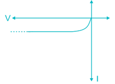
From the figure it is clear that the reverse current is independent of voltage.
The gain of a CE amplifier is highest at- a)Low frequencies
- b)Mid frequencies
- c)High frequencies
- d)All frequencies
Correct answer is option 'B'. Can you explain this answer?
The gain of a CE amplifier is highest at
a)
Low frequencies
b)
Mid frequencies
c)
High frequencies
d)
All frequencies
|
|
Rounak Rane answered |
A common emitter amplifier acts as a bandpass amplifier due to reduced gain at low and high frequencies. This is due to source, emitter and parasitic capacitances.
In a bipolar junction transistor, the current gain β.- a)Does not change with the change in temperature
- b)Increases exponentially with the increase in temperature
- c)Decreases with the increase in temperature
- d)Increases with the increase in temperature
Correct answer is option 'D'. Can you explain this answer?
In a bipolar junction transistor, the current gain β.
a)
Does not change with the change in temperature
b)
Increases exponentially with the increase in temperature
c)
Decreases with the increase in temperature
d)
Increases with the increase in temperature
|
|
Prisha Kulkarni answered |
The current gain β is defined as 
At higher temperatures the thermal injection increases the collector current & hence β increases.
Which among the following will possess a higher bandwidth, if two transistors are provided with unity gain frequency?- a)Transistor with lower hfe
- b)Transistor with higher hfe
- c)Transistor with lower hre
- d)Transistor with higher hre
Correct answer is option 'A'. Can you explain this answer?
Which among the following will possess a higher bandwidth, if two transistors are provided with unity gain frequency?
a)
Transistor with lower hfe
b)
Transistor with higher hfe
c)
Transistor with lower hre
d)
Transistor with higher hre
|
|
Ananya Sharma answered |
In transistor the Gain Bandwidth product is equal to unity, since gain is proportional to DC current gain hfe the transistor with lower hfe will have higher bandwidth.
What is the required connection for an enhancement type N-MOSFET to function as a resistor?- a)Gate connected to source
- b)Gate connected to drain
- c)Drain connected to source
- d)Drain voltage should be less than the overdrive voltage
Correct answer is option 'B'. Can you explain this answer?
What is the required connection for an enhancement type N-MOSFET to function as a resistor?
a)
Gate connected to source
b)
Gate connected to drain
c)
Drain connected to source
d)
Drain voltage should be less than the overdrive voltage
|
|
Athul Banerjee answered |
The overdrive voltage is defined as the voltage between transistor gate and source (VGS) in excess of the threshold voltage (VT) ie Vgs - Vt
For N-Mos to function as a resistor, it should be operated in linear region. I.e. VDS < Vgs – Vt
For using N-Mos as an amplifier, it should be operated in saturation region. I.e. VDS ≥ Vgs – Vt
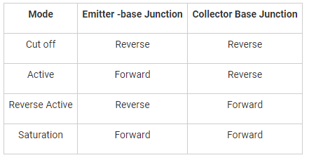
For a transistor to act as current amplifier.- a)Both its emitter base junction and collector-base junction are forward biased
- b)Both its emitter base junction and collector base thin junction are reverse biased
- c)Its emitter base junction is forward biased while collector base junction is reverse biased
- d)Its emitter base junction is reverse biased while collector base junction is forward biased
Correct answer is option 'C'. Can you explain this answer?
For a transistor to act as current amplifier.
a)
Both its emitter base junction and collector-base junction are forward biased
b)
Both its emitter base junction and collector base thin junction are reverse biased
c)
Its emitter base junction is forward biased while collector base junction is reverse biased
d)
Its emitter base junction is reverse biased while collector base junction is forward biased
|
|
Samridhi Bose answered |
For any amplification, (voltage or current), the transistor should be operated in active region ie. emitter base junction is forward biased and collector base junction is reverse biased
A light-emitting diode (LED) converts:- a)Sound energy into optical signal
- b)Optical signal into thermal energy
- c)Thermal energy into electrical signal
- d)electrical current into optical signal
Correct answer is option 'D'. Can you explain this answer?
A light-emitting diode (LED) converts:
a)
Sound energy into optical signal
b)
Optical signal into thermal energy
c)
Thermal energy into electrical signal
d)
electrical current into optical signal
|
|
Avik Iyer answered |
LED works on the principle of electroluminescence which is emission of light under influence of electric field.
In an amplifier the maximum power transfer to the load resistance should be- a)As small as possible
- b)As large as possible
- c)Equal to the value of the input resistance of the amplifier
- d)Equal to the value of the output impedance
Correct answer is option 'D'. Can you explain this answer?
In an amplifier the maximum power transfer to the load resistance should be
a)
As small as possible
b)
As large as possible
c)
Equal to the value of the input resistance of the amplifier
d)
Equal to the value of the output impedance

|
Arjun Menon answered |
In an amplifier the maximum power is transferred to the load when the load resistance is equal to output impedance of amplifier
In a p-n Junction with no externally applied voltage, the drift and diffusion components of the hole and electron currents:- a)Must sum to zero separately
- b)Must sum to unity separately
- c)Must sum to zero
- d)Must sum to unity
Correct answer is option 'C'. Can you explain this answer?
In a p-n Junction with no externally applied voltage, the drift and diffusion components of the hole and electron currents:
a)
Must sum to zero separately
b)
Must sum to unity separately
c)
Must sum to zero
d)
Must sum to unity
|
|
Bijoy Mehta answered |
In a p-n Junction when no bias voltage is applied, the net current is zero.
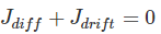
Hence the drift and diffusion components of the hole and electron currents must sum to zero.
Generally, mobility of electrons in semiconductor is _________ times the mobility of holes:- a)Two
- b)Three
- c)Four
- d)Five
Correct answer is option 'B'. Can you explain this answer?
Generally, mobility of electrons in semiconductor is _________ times the mobility of holes:
a)
Two
b)
Three
c)
Four
d)
Five
|
|
Aaditya Choudhary answered |
Mobility of Electrons in Semiconductors
The mobility of electrons and holes in a semiconductor is an important factor that determines the efficiency and performance of electronic devices. The mobility of a charge carrier refers to its ability to move in response to an electric field. In semiconductors, both electrons and holes contribute to the overall electrical conductivity.
Explanation:
Mobility of Electrons
- Electrons are negatively charged carriers in a semiconductor material.
- They have the ability to move freely through the crystal lattice when an electric field is applied.
- The mobility of electrons is determined by various factors such as scattering mechanisms, crystal structure, temperature, and impurity concentrations.
- In general, the mobility of electrons in a semiconductor is higher than the mobility of holes.
Mobility of Holes
- Holes are the absence of an electron in the valence band and can be thought of as positive charge carriers.
- When an electron moves from the valence band to the conduction band, it leaves behind a hole in the valence band.
- Holes can move through the crystal lattice by the motion of surrounding electrons filling the hole.
- The mobility of holes is generally lower than the mobility of electrons due to their lower effective mass and higher scattering rates.
Ratio of Mobility
- The ratio of mobility of electrons to holes in a semiconductor is dependent on the specific material and its properties.
- It is generally observed that the mobility of electrons is approximately three times higher than the mobility of holes.
- This means that electrons can move more easily and quickly through the semiconductor compared to holes when an electric field is applied.
Importance
- The mobility of charge carriers is a crucial parameter in the design and optimization of semiconductor devices.
- It affects the speed, power consumption, and overall performance of devices such as transistors, diodes, and integrated circuits.
- Higher mobility of charge carriers allows for faster switching speeds and improved device efficiency.
In conclusion, the mobility of electrons in a semiconductor is generally three times higher than the mobility of holes. This knowledge is important in understanding the behavior of charge carriers in semiconductors and designing efficient electronic devices.
What are the ON/OFF terminals of a transistor when it is operated as a switch?- a)Collector to base
- b)Collector to emitter
- c)Base to collector
- d)Emitter to base
Correct answer is option 'B'. Can you explain this answer?
What are the ON/OFF terminals of a transistor when it is operated as a switch?
a)
Collector to base
b)
Collector to emitter
c)
Base to collector
d)
Emitter to base
|
|
Prashanth Mehra answered |
Transistor switches can be used to switch low DC voltages ON or OFF by operating it in saturation or cut-off mode
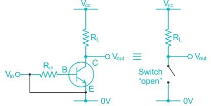
The CE terminals act as ON/OFF terminals as shown in figure above.
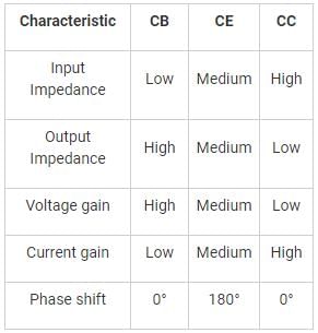
A transistor connected in common base configuration has:- a)A high input resistance and low output resistance
- b)A high input resistance and high output resistance
- c)A low input resistance and high output resistance
- d)A low input resistance and low output resistance
Correct answer is option 'C'. Can you explain this answer?
A transistor connected in common base configuration has:
a)
A high input resistance and low output resistance
b)
A high input resistance and high output resistance
c)
A low input resistance and high output resistance
d)
A low input resistance and low output resistance
|
|
Gargi Basak answered |
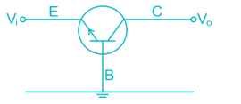
Input Terminal Emitter – Base (EB)
Output Terminal Collector – Base (CB)
Since for Amplification Application in BJT
EB Junction → Forward Biased (Low Impedance)
CB Junction → Reversed Biased (High Impedance)
Input Impedance is low
Output Impedance is high
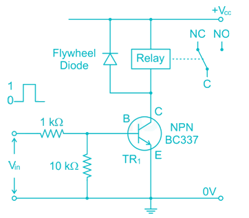
In an electronic circuit transistor is used for switching ON and OFF a relay when the transistor switches OFF the relay a higher voltage appears across the transistor. How can a transistor be protected from this voltage?- a)A capacitor in series to the relay
- b)A resistor in series to the relay
- c)An inductor parallel to the relay
- d)A diode parallel to the relay
Correct answer is option 'D'. Can you explain this answer?
In an electronic circuit transistor is used for switching ON and OFF a relay when the transistor switches OFF the relay a higher voltage appears across the transistor. How can a transistor be protected from this voltage?
a)
A capacitor in series to the relay
b)
A resistor in series to the relay
c)
An inductor parallel to the relay
d)
A diode parallel to the relay
|
|
Gitanjali Chauhan answered |
In transistor relay circuit when relay is in OFF state, high reverse voltage is developed across relay terminals, this can damage the transistor. Hence a diode is connected parallel to the relay, this clamps the voltage across the relay and helps dissipate the energy in diode.
at room temperature intrinsic carrier concentration is higher in germanium than in silicon because __________.- a)Carrier mobilities are higher Ge than in Si
- b)energy gap in Ge is smaller than that in Si
- c)Atomic number of Ge is larger than in Si
- d)Atomic weight of Ge is larger than in Si
Correct answer is option 'B'. Can you explain this answer?
at room temperature intrinsic carrier concentration is higher in germanium than in silicon because __________.
a)
Carrier mobilities are higher Ge than in Si
b)
energy gap in Ge is smaller than that in Si
c)
Atomic number of Ge is larger than in Si
d)
Atomic weight of Ge is larger than in Si
|
|
Prisha Kulkarni answered |
Carrier concentrations depends on the energy gap in the intrinsic semiconductor. In the case of Ge and Si the intrinsic carrier concentration of Ge is higher than that of Si because the energy gap in Ge is smaller than that of Si.
Which diode has negative resistance region in its characteristics?- a)Photodiode
- b)Tunnel diode
- c)Varactor diode
- d)Zener diode
Correct answer is option 'B'. Can you explain this answer?
Which diode has negative resistance region in its characteristics?
a)
Photodiode
b)
Tunnel diode
c)
Varactor diode
d)
Zener diode
|
|
Manoj Mehra answered |
Tunnel diode characteristics
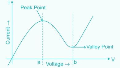
In Region between Peak Point & valley Point the current in Tunnel diode decrease with increase in forward Bias voltage. Thus Tunnel diode shows -ve resistance between peak point & valley point
Transistors leakage current mainly depends on:- a)Doping of base
- b)Size of emitter
- c)Rating of transistor
- d)Temperature
Correct answer is option 'D'. Can you explain this answer?
Transistors leakage current mainly depends on:
a)
Doping of base
b)
Size of emitter
c)
Rating of transistor
d)
Temperature
|
|
Bijoy Mehta answered |
Transistor leakage current refers to the small amount of current that flows through a transistor even when it is in the off state. This leakage current can have a significant impact on the overall performance and efficiency of a transistor.
The leakage current mainly depends on the temperature of the transistor. However, other factors like the doping of the base, size of the emitter, and rating of the transistor can also have some influence on the leakage current.
1. Temperature:
The temperature of the transistor is a critical factor that affects the leakage current. As the temperature increases, the energy level of the electrons in the base region also increases. This results in a higher probability of electrons crossing the base-emitter junction and causing a leakage current. Therefore, higher temperatures lead to higher leakage currents.
2. Doping of the base:
The doping of the base region also affects the leakage current. The base region is typically lightly doped compared to the emitter and collector regions. If the base doping concentration is too high, it can lead to an increase in the leakage current. This is because a higher doping concentration increases the probability of electrons crossing the base-emitter junction, even in the off state.
3. Size of the emitter:
The size of the emitter can indirectly affect the leakage current. A larger emitter area provides more space for electrons to cross the base-emitter junction, leading to a higher leakage current. However, the size of the emitter is usually chosen based on other performance requirements, and optimizing it solely for reducing leakage current may not be practical.
4. Rating of the transistor:
The rating of the transistor, such as its breakdown voltage and maximum operating temperature, can also influence the leakage current. Transistors with higher breakdown voltages and higher temperature ratings tend to have lower leakage currents. This is because these transistors are designed to operate under more stringent conditions, which also helps reduce leakage current.
In summary, while the temperature of the transistor is the primary factor affecting leakage current, other factors like the doping of the base, size of the emitter, and rating of the transistor can also have some influence. It is important to consider these factors during the design and selection of transistors to minimize leakage current and optimize overall performance.
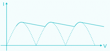
A centre tapped full wave rectifier output contains only-- a)Even harmonics
- b)Odd harmonics
- c)Even and Odd harmonics
- d)No harmonics
Correct answer is option 'A'. Can you explain this answer?
A centre tapped full wave rectifier output contains only-
a)
Even harmonics
b)
Odd harmonics
c)
Even and Odd harmonics
d)
No harmonics
|
|
Upasana Joshi answered |
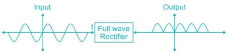
Since the output of full wave rectifier is an even function. Hence from Fourier series Analysis we know that even function have even harmonics thus output of FWR contains only even harmonics.
Which of the following is a bipolar device?- a)Tunnel diode
- b)Gunn diode
- c)FET
- d)UJT
Correct answer is option 'A'. Can you explain this answer?
Which of the following is a bipolar device?
a)
Tunnel diode
b)
Gunn diode
c)
FET
d)
UJT
|
|
Srestha Gupta answered |
Gunn diode, FET and UJT are unipolar devices in which current is due to only one type of carrier. While tunnel diode is bipolar device in which both electrons and holes contribute to current.
A Schottky diode is a- a)Both majority and minority carrier diode
- b)Majority carrier device
- c)Minority carrier device
- d)Fast recovery diode
Correct answer is option 'B'. Can you explain this answer?
A Schottky diode is a
a)
Both majority and minority carrier diode
b)
Majority carrier device
c)
Minority carrier device
d)
Fast recovery diode
|
|
Mihir Khanna answered |
It is a majority carrier device. It is a semiconductor diode with a very fast switching action, but a low forward voltage drop. When a current flows through the diode there is a small voltage drop across the diode terminals. In a normal diode, the voltage drop is between 0.6 to 1.7 volts, while in a Schottky diode the voltage drop normally ranges between 0.15 and 0.45volts. This lower voltage drop provides higher switching speed and better system efficiency.
In Schottky diode, a semiconductor-metal junction is formed between a semiconductor and a metal, thus creating a Schottky barrier. The N-type semiconductor acts as a cathode and the metal side acts as the anode of the diode. The Schottky barrier diode is a unidirectional device conducting current flows only in one direction.
The LED emits light of a particular colour because- a)It is fabricated from a fluorescent material
- b)Transition between energy levels of the carriers takes place while crossing the p-n junction
- c)Heat generated in the diode is converted into light
- d)The band gap of the semiconductor material used in the fabrication of the diode is equal to the energy hν of the light photon
Correct answer is option 'D'. Can you explain this answer?
The LED emits light of a particular colour because
a)
It is fabricated from a fluorescent material
b)
Transition between energy levels of the carriers takes place while crossing the p-n junction
c)
Heat generated in the diode is converted into light
d)
The band gap of the semiconductor material used in the fabrication of the diode is equal to the energy hν of the light photon
|
|
Lekshmi Rane answered |
LEDs are fabricated using direct bandgap semiconductors.In which, when electron transfers from conductor band to valence band and recombines with the holes the energy difference between the both bandsget converted in to light with frequency ‘ν’, it is related with energy as,
E = hν, where h is Planck’s constant.
UJT are used in- a)Only timing circuits
- b)Only oscillator circuits
- c)Only bi-stable circuits
- d)In all the circuits
Correct answer is option 'D'. Can you explain this answer?
UJT are used in
a)
Only timing circuits
b)
Only oscillator circuits
c)
Only bi-stable circuits
d)
In all the circuits
|
|
Isha Singh answered |
Uni Junction Transistor is a three terminal semiconductor device formed by single P-N junction. It functions as an ON-OFF switch and has unidirectional conductivity and negative resistance characteristics.
It is used to trigger SCR devices and used in relaxation oscillator.
The capacitance of a p-n junction diode:- a)Does not change with the increase in the forward bias voltage
- b)Decrease with the increase in the forward bias voltage
- c)Increase exponentially with the increases in the forward bias voltage
- d)Increase linearly with the increase in the forward bias voltage
Correct answer is option 'C'. Can you explain this answer?
The capacitance of a p-n junction diode:
a)
Does not change with the increase in the forward bias voltage
b)
Decrease with the increase in the forward bias voltage
c)
Increase exponentially with the increases in the forward bias voltage
d)
Increase linearly with the increase in the forward bias voltage
|
|
Aman Datta answered |
Understanding Capacitance in a P-N Junction Diode
The capacitance of a p-n junction diode is a crucial parameter that is influenced by the voltage applied across the junction. The behavior of this capacitance under forward bias is significant for various applications in electronics.
Forward Bias and Depletion Region
- When a p-n junction diode is forward-biased, the applied voltage reduces the width of the depletion region.
- As the depletion region narrows, more charge carriers (holes and electrons) are able to recombine, leading to an increase in capacitance.
Capacitance and Forward Bias Relationship
- The capacitance of the diode is related to the charge stored in the depletion region. As the forward bias voltage increases, the charge density increases.
- This results in a higher capacitance due to the effective area of the junction increasing as more charge carriers are available.
Exponential Increase in Capacitance
- The increase in capacitance with forward bias is not linear; it tends to be exponential.
- This is because the charge carrier injection into the depletion region increases rapidly as the voltage rises, leading to a significant change in capacitance.
Conclusion
Therefore, the correct answer is that the capacitance of a p-n junction diode increases exponentially with the increase in forward bias voltage. This characteristic is vital for understanding how diodes operate in various circuits, especially in high-frequency applications and signal processing.
A tuned amplifier is used:- a)In audio amplification
- b)For noise removal in radio signals
- c)In radio receivers
- d)None of the above
Correct answer is option 'C'. Can you explain this answer?
A tuned amplifier is used:
a)
In audio amplification
b)
For noise removal in radio signals
c)
In radio receivers
d)
None of the above
|
|
Prisha Kulkarni answered |
Tuned amplifiers are employed for the purpose of selecting a particular frequency among set of available frequencies. Hence they are employed in radio receives.
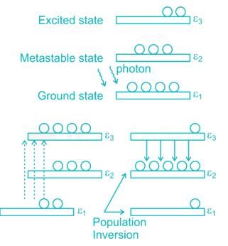
Semiconductor lasers are based on the following principle:- a)Population inversion at a junction
- b)PN junction is formed between degenerate materials
- c)Use of negative conductance devices
- d)Tunnelling phenomena
Correct answer is option 'A'. Can you explain this answer?
Semiconductor lasers are based on the following principle:
a)
Population inversion at a junction
b)
PN junction is formed between degenerate materials
c)
Use of negative conductance devices
d)
Tunnelling phenomena
|
|
Tanvi Rane answered |
LASER stands for Light Amplification by Stimulated Emission of Radiation. These are based on the principle of population inversion at a junction as explained in below figure
The h-parameter equivalent circuit of a BJT is valid for:- a)Large signal operation at high frequencies
- b)Small signal operation at low frequencies
- c)Large signal operation at low frequencies
- d)Small signal operation at high frequencies
Correct answer is option 'B'. Can you explain this answer?
The h-parameter equivalent circuit of a BJT is valid for:
a)
Large signal operation at high frequencies
b)
Small signal operation at low frequencies
c)
Large signal operation at low frequencies
d)
Small signal operation at high frequencies
|
|
Dhruv Datta answered |
The h-parameter equivalent circuit of a Bipolar Junction Transistor (BJT) is a simplified model that represents the transistor's behavior in terms of its hybrid parameters, also known as h-parameters. These parameters are used to describe the relationship between the voltage and current at the BJT terminals.
The h-parameter equivalent circuit consists of three elements: the current source hfe (also known as the forward current transfer ratio or beta), the input impedance hie, and the output impedance hoe. It assumes that the BJT is operating in the active region, where the transistor acts as an amplifier.
The validity of the h-parameter equivalent circuit depends on the operating conditions of the BJT. Let's consider the given options to determine the correct answer:
a) Large signal operation at high frequencies:
The h-parameter equivalent circuit is not valid for large signal operation because it assumes small signal conditions. Large signal operation refers to situations where the signal amplitudes are significant enough to cause non-linear effects in the transistor's behavior. At high frequencies, the BJT's parasitic capacitances also become significant, which are not considered in the h-parameter model.
c) Large signal operation at low frequencies:
Similar to option a, the h-parameter circuit is not suitable for large signal operation, regardless of the frequency. The h-parameter model assumes small signal conditions, where the signal amplitudes are small enough to avoid non-linear effects.
d) Small signal operation at high frequencies:
While the h-parameter circuit assumes small signal conditions, it does not accurately represent the BJT's behavior at high frequencies. At high frequencies, the transistor's parasitic capacitances and other high-frequency effects become significant, which are not considered in the h-parameter model.
b) Small signal operation at low frequencies:
The h-parameter equivalent circuit is most valid for small signal operation at low frequencies. In this operating region, the signal amplitudes are small enough to avoid non-linear effects, and the parasitic capacitances and other high-frequency effects are negligible. Therefore, the h-parameter model provides a reasonably accurate representation of the BJT's behavior in this operating region.
In conclusion, the h-parameter equivalent circuit of a BJT is valid for small signal operation at low frequencies. It provides a simplified yet effective model for analyzing the transistor's behavior in this operating region.
The ripple factor of a power supply is a measure of- a)Its filter efficiency
- b)Its voltage regulation
- c)Its purity of output
- d)Diode rating
Correct answer is option 'C'. Can you explain this answer?
The ripple factor of a power supply is a measure of
a)
Its filter efficiency
b)
Its voltage regulation
c)
Its purity of output
d)
Diode rating
|
|
Dishani Bose answered |
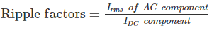
Thus if the ripple factor is less, the power supply has less AC components and power supply output is more pure (i.e more DC without much fluctuations)
Thus ripple factor is indication of purity of output of power supply
The upper cut-off frequency of an RC coupled amplifier mainly depends upon:- a)Output capacitance of signal source
- b)Inter-electrode and stray shunt capacitances
- c)Coupling capacitor
- d)Emitter bypass capacitor
Correct answer is option 'C'. Can you explain this answer?
The upper cut-off frequency of an RC coupled amplifier mainly depends upon:
a)
Output capacitance of signal source
b)
Inter-electrode and stray shunt capacitances
c)
Coupling capacitor
d)
Emitter bypass capacitor
|
|
Tanishq Chauhan answered |
The Upper cut off frequency of R-C coupled multistage Amplifier is
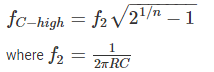
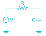
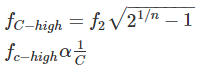
Thus upper – cut off frequency depends on coupling capacitors
Transistor biasing is done to keep _______ in the circuit.- a)Proper direct current
- b)Proper alternating current
- c)The base current small
- d)Collector current small
Correct answer is option 'A'. Can you explain this answer?
Transistor biasing is done to keep _______ in the circuit.
a)
Proper direct current
b)
Proper alternating current
c)
The base current small
d)
Collector current small
|
|
Sakshi Tiwari answered |
Biasing of a transistor is done to keep the stable DC condition like VBE, IC needed for specific action of transistor, like amplification, switch, etc.
The bonding forces in compound semiconductors, such as GaAs, arise form- a)Ionic bonding
- b)Metallic bonding
- c)Covalent bonding
- d)Combination of ironic and covalent bonding
Correct answer is option 'C'. Can you explain this answer?
The bonding forces in compound semiconductors, such as GaAs, arise form
a)
Ionic bonding
b)
Metallic bonding
c)
Covalent bonding
d)
Combination of ironic and covalent bonding
|
|
Mihir Chawla answered |
In semiconductors like GaAs the elements Ga and As are in covalent bond. Arsenic has five valence electrons while gallium has three valence electrons. Therefore, in GaAs crystal Arsenic contribute one electron to Gallium and it is shared between both atoms in a covalent bond
Two p-n junction diodes are connected back to back to make a transistor. Which one of the following is correct?- a)The current gain of such a transistor will be high
- b)The current gain of such a transistor will be moderate
- c)It cannot be used as a transistor due to large base width
- d)It can be used only for p-n-p transistor
Correct answer is option 'C'. Can you explain this answer?
Two p-n junction diodes are connected back to back to make a transistor. Which one of the following is correct?
a)
The current gain of such a transistor will be high
b)
The current gain of such a transistor will be moderate
c)
It cannot be used as a transistor due to large base width
d)
It can be used only for p-n-p transistor
|
|
Aniket Choudhury answered |
A transistor operation needs very small base width to allow the minority carriers, drifted from emitter to diffuse into collector.
By connecting two PN diodes back to back the transistor will have wide base causing the minority carriers from emitter to recombine in base region before they diffuse into collector. This reduces collector current or cut off entirely.
What is the main source of distortion in a push-pull amplifier?- a)Fundamental component
- b)Second harmonic
- c)Third harmonic
- d)All even harmonics
Correct answer is option 'C'. Can you explain this answer?
What is the main source of distortion in a push-pull amplifier?
a)
Fundamental component
b)
Second harmonic
c)
Third harmonic
d)
All even harmonics
|
|
Maulik Das answered |
In push-pull amplifiers each transistor operates only for one half cycle of AC voltage, in it even harmonics are minimised, so distortion is mainly due to odd harmonics.
Hence of the given options third harmonics needs to be eliminated
In the silicon crystal structure, the recombination rate is proportional to the number of;- a)Free electrons and holes
- b)Covalent bonds
- c)Free electrons
- d)Free holes
Correct answer is option 'A'. Can you explain this answer?
In the silicon crystal structure, the recombination rate is proportional to the number of;
a)
Free electrons and holes
b)
Covalent bonds
c)
Free electrons
d)
Free holes
|
|
Nandita Kulkarni answered |
Recombination Rate in Silicon Crystal Structure
Introduction:
Silicon is a semiconductor material that is widely used in electronics. In its crystal structure, the recombination rate is an important parameter that affects the performance of electronic devices. Recombination refers to the process by which free electrons and holes combine, leading to the release of energy in the form of photons or heat. The rate of recombination is proportional to the number of free electrons and holes in the crystal.
Proportional to the Number of Electrons and Holes:
The recombination rate in a silicon crystal is proportional to the number of free electrons and holes. This is because recombination occurs when free electrons and holes come into contact with each other. The more free electrons and holes there are in the crystal, the more likely they are to come into contact and recombine.
Covalent Bonds:
Covalent bonds are the chemical bonds that hold the silicon atoms together in the crystal. They are formed by the sharing of electrons between adjacent atoms. Covalent bonds do not directly affect the recombination rate in the crystal.
Free Electrons:
Free electrons are electrons that are not bound to any atom in the crystal. They are created when silicon is doped with impurities such as phosphorus. Free electrons contribute to the conductivity of the crystal and are also involved in the recombination process.
Free Holes:
Free holes are vacant spaces in the crystal lattice where an electron is missing. They are created when silicon is doped with impurities such as boron. Free holes also contribute to the conductivity of the crystal and are involved in the recombination process.
Conclusion:
In conclusion, the recombination rate in a silicon crystal is proportional to the number of free electrons and holes. The covalent bonds that hold the crystal together do not directly affect the recombination rate. Understanding the recombination rate is important for the design and optimization of electronic devices based on silicon.
In a rectifier, commutation of diodes refers to transferring energy from –- a)Rectifier diode to load
- b)Freewheeling diode to load
- c)Freewheeling diode to rectifier diode
- d)Rectifier diode to freewheeling diode
Correct answer is option 'D'. Can you explain this answer?
In a rectifier, commutation of diodes refers to transferring energy from –
a)
Rectifier diode to load
b)
Freewheeling diode to load
c)
Freewheeling diode to rectifier diode
d)
Rectifier diode to freewheeling diode
|
|
Bijoy Mehta answered |
Commutation in a rectifier is the process of transfer of current from one device (diode or thyristor) to the other in a rectifier. The device from which the current is transferred is called the outgoing device and the device to which the current is transferred is called the incoming device. The incoming device turns on at the beginning of commutation while the outgoing device turns off at the end of commutation.
Here, commutation of diodes refers to transferring energy from rectifier diode to freewheeling diode. Freewheeling diode is used to reduce the harmonics and also suppress the voltage spikes occur in inductive load.
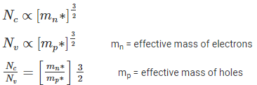
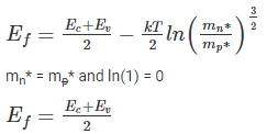
The Fermi level EF in an intrinsic semiconductor, if effective masses of holes and electrons are same is:- a)EC - EV
- b)EC + EV
- c)

- d)

Correct answer is option 'C'. Can you explain this answer?
The Fermi level EF in an intrinsic semiconductor, if effective masses of holes and electrons are same is:
a)
EC - EV
b)
EC + EV
c)
d)
|
|
Shivam Das answered |
The fermi level (EF) in an intrinsic semiconductor is given by
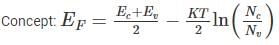
Where Ec = Energy of conduction band minima
Ev = Energy of valence band maxima
K = Boltzman constant
T = Temperature
Nc = density of states in conduction band
Nv = density of states in valence band
In a BJT, collector region width is maximum when it.1. Collects maximum number of charge carrier2. Reduces heat dissipation per unit area Out of these- a)Only 1 is correct
- b)Only 2 is correct
- c)Both 1 and 2 are correct
- d)Neither 1 nor 2 incorrect
Correct answer is option 'C'. Can you explain this answer?
In a BJT, collector region width is maximum when it.
1. Collects maximum number of charge carrier
2. Reduces heat dissipation per unit area Out of these
a)
Only 1 is correct
b)
Only 2 is correct
c)
Both 1 and 2 are correct
d)
Neither 1 nor 2 incorrect
|
|
Alok Roy answered |
The order of width is
wcollector > wemitter > wBase
The order of doping is
nemitter > ncollector > nbase
At much lower temperature, semiconductors behave as:- a)Semiconductors only
- b)Conductors
- c)Insulators
- d)Conductors or insulator
Correct answer is option 'C'. Can you explain this answer?
At much lower temperature, semiconductors behave as:
a)
Semiconductors only
b)
Conductors
c)
Insulators
d)
Conductors or insulator
|
|
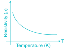
Ashwin Mukherjee answered |
At lower temperatures, the electrons in valence band do not have sufficient energy to jump into conduction band. Thus carrier concentration decreases at lower temperatures and semiconductors behaves as insulators
Chapter doubts & questions for Basic Electronics - Mock Test Series for SSC JE Electrical Engineering 2026 2025 is part of Electrical Engineering (EE) exam preparation. The chapters have been prepared according to the Electrical Engineering (EE) exam syllabus. The Chapter doubts & questions, notes, tests & MCQs are made for Electrical Engineering (EE) 2025 Exam. Find important definitions, questions, notes, meanings, examples, exercises, MCQs and online tests here.
Chapter doubts & questions of Basic Electronics - Mock Test Series for SSC JE Electrical Engineering 2026 in English & Hindi are available as part of Electrical Engineering (EE) exam.
Download more important topics, notes, lectures and mock test series for Electrical Engineering (EE) Exam by signing up for free.
Mock Test Series for SSC JE Electrical Engineering 2026
2 videos|1 docs|55 tests
|
|
© EduRev
|
Education Revolution
|


|


Signup to see your scores
go up within 7 days!
Access 1000+ FREE Docs, Videos and Tests
Takes less than 10 seconds to signup