


All Exams >
GATE Physics >
Electronics for GATE >
All Questions
All questions of Operational Amplifier for GATE Physics Exam
When negative feedback is used, then the gain bandwidth product of an Op-Amp.- a)fluctuates
- b)increases
- c)decreases
- d)stays the same
Correct answer is option 'D'. Can you explain this answer?
When negative feedback is used, then the gain bandwidth product of an Op-Amp.
a)
fluctuates
b)
increases
c)
decreases
d)
stays the same
|
|
Jayant Mishra answered |
Applying the feedback will reduce the gain but increase the bandwidth hence, the gain bandwidth product = Av x f. he remains constant for any voltage feedback amplifier.
The correct answer is: stays the same
The correct answer is: stays the same

Ideal op-amp has infinite voltage gain because - a)To control the output voltage
- b)To obtain finite output voltage
- c)To receive zero noise output voltage
- d)None of the mentioned
Correct answer is option 'B'. Can you explain this answer?
Ideal op-amp has infinite voltage gain because
a)
To control the output voltage
b)
To obtain finite output voltage
c)
To receive zero noise output voltage
d)
None of the mentioned
|
|
Vedika Singh answered |
As the voltage gain is infinite, the voltage between the inverting and non-inverting terminal (i.e. differential input voltage) is essentially zero for finite output voltage.
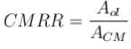
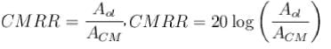
If Av(d) = 3500 and ACM = 0.35, then CMRR is :- a)1225
- b)10000
- c)40 dB
- d)80 dB
Correct answer is option 'B,D'. Can you explain this answer?
If Av(d) = 3500 and ACM = 0.35, then CMRR is :
a)
1225
b)
10000
c)
40 dB
d)
80 dB
|
|
Jayant Mishra answered |
The solution to your question is:
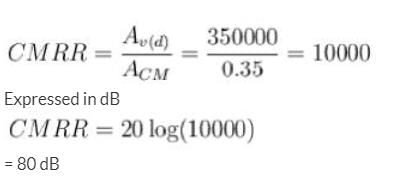
Hence, The correct answers are: 10000, 80 dB

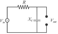
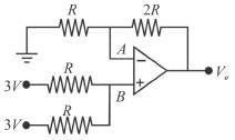
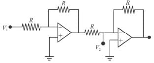
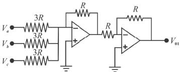
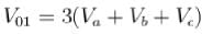
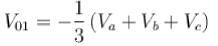
A non-inverting Op-Amp summer is shown in the figure. The output voltage V0 is
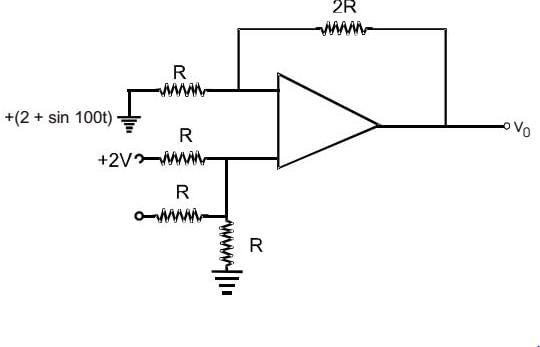
- a)Sin 100t
- b)2 Sin 100t
- c)3 Sin 100t
- d)3/2 Sin 100t
Correct answer is option 'C'. Can you explain this answer?
A non-inverting Op-Amp summer is shown in the figure. The output voltage V0 is
a)
Sin 100t
b)
2 Sin 100t
c)
3 Sin 100t
d)
3/2 Sin 100t

|
Pie Academy answered |
V0
= -2(1 + 2R/R) + (2 + sin 100 t)(1 + 2R/R)= – 6 + 6 + 3 sin 100 t
= 3 sin 100 t
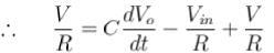
In an integrator, the feedback element is a :- a)zener diode
- b)voltage divider
- c)register
- d)capacitor
Correct answer is option 'D'. Can you explain this answer?
In an integrator, the feedback element is a :
a)
zener diode
b)
voltage divider
c)
register
d)
capacitor
|
|
Jayant Mishra answered |
Integrator circuit is as shown below
The correct answer is: capacitor
The correct answer is: capacitor
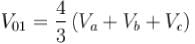
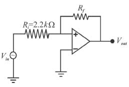
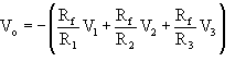
For the amplifier shown in figure
- a)The average of the input values is the same magnitude as Vout but of opposite sign
- b)The average of the input values is the different magnitude as Vout with opposite sign
- c)The average of the input values is of the different magnitude as Vout with same sign
- d)The average of the input values is the same magnitudes as Vout of the same sign
Correct answer is option 'A'. Can you explain this answer?
For the amplifier shown in figure
a)
The average of the input values is the same magnitude as Vout but of opposite sign
b)
The average of the input values is the different magnitude as Vout with opposite sign
c)
The average of the input values is of the different magnitude as Vout with same sign
d)
The average of the input values is the same magnitudes as Vout of the same sign
|
|
Jayant Mishra answered |
Since the input resistors are equal;
R= 100/kΩ
The output voltage is
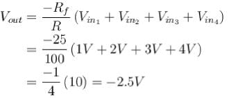
Whereas, the input average
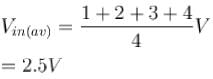
Shows that average of the input value is the same magnitude as Vout but of opposite sign.
The correct answer is: The average of the input values is the same magnitude as Vout but of opposite sign
R= 100/kΩ
The output voltage is
Whereas, the input average
Shows that average of the input value is the same magnitude as Vout but of opposite sign.
The correct answer is: The average of the input values is the same magnitude as Vout but of opposite sign
In the differentiating circuit given in the figure, the function of R1 is to:

- a)Present oscillations at high frequency.
- b)Eliminate high frequency noise spikes
- c)Maintain high input impedance
- d)Enable circuit to approach ideal differentiator
Correct answer is option 'C'. Can you explain this answer?
In the differentiating circuit given in the figure, the function of R1 is to:
a)
Present oscillations at high frequency.
b)
Eliminate high frequency noise spikes
c)
Maintain high input impedance
d)
Enable circuit to approach ideal differentiator
|
|
Pie Academy answered |
R1 maintains the high input impedance.
The correct answer is: Maintain high input impedance
The correct answer is: Maintain high input impedance
What is the minimum voltage required to make the PN junction of a real silicon transistor in forward biased?
Correct answer is '0.7'. Can you explain this answer?
What is the minimum voltage required to make the PN junction of a real silicon transistor in forward biased?
|
|
Pooja Choudhury answered |
0.7 volts is the minimum voltage required to make the PN junction of a real silicon transistor in forward biased. This 0.7 volt potential difference makes the PN junction between base and emitter terminal in forward biased.
A certain Op-Amp has bias currents of 50μA and 49.3μA. The input offset current is (in nA).
Correct answer is '700'. Can you explain this answer?
A certain Op-Amp has bias currents of 50μA and 49.3μA. The input offset current is (in nA).

|
Akanksha Choudhary answered |
The input offset current is the different of input bias currents i.e.
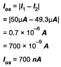
The correct answer is: 700
The correct answer is: 700
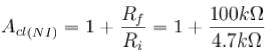
If the voltage gain for each input of a summing amplifier with a 4.7 kΩ feedback resistor is unity, the input resistors must have a value of (in kΩ?
Correct answer is '4.7'. Can you explain this answer?
If the voltage gain for each input of a summing amplifier with a 4.7 kΩ feedback resistor is unity, the input resistors must have a value of (in kΩ?
|
|
Pragati Sharma answered |
Voltage gain for each
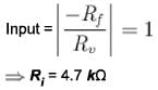
The correct answer is: 4.7
The correct answer is: 4.7
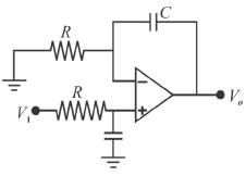
The circuit shown in the figure can be used as a
- a)high pass filter
- b)low pass filter
- c)differentiator
- d)Integrator
Correct answer is option 'B,D'. Can you explain this answer?
The circuit shown in the figure can be used as a
a)
high pass filter
b)
low pass filter
c)
differentiator
d)
Integrator
|
|
Jayant Mishra answered |
The given circuit is

It is an integrator and low-pass filter.
The correct answers are: low pass filter, Integrator
It is an integrator and low-pass filter.
The correct answers are: low pass filter, Integrator
A differential amplifier.- a)is a part of an Op-Amp
- b)has one input only
- c)has two output
- d)has one input and one output
Correct answer is option 'A,C'. Can you explain this answer?
A differential amplifier.
a)
is a part of an Op-Amp
b)
has one input only
c)
has two output
d)
has one input and one output
|
|
Jayant Mishra answered |
Any differential amplifier has two inputs and two outputs (one is Vout and other is ground potential) The correct answers are: is a part of an Op-Amp, has two output
Phase shifts through an Op -Amp is caused by.- a)the gain Roll-off
- b)the internal RC circuit
- c)negative feedback
- d)the external RC circuit
Correct answer is option 'B'. Can you explain this answer?
Phase shifts through an Op -Amp is caused by.
a)
the gain Roll-off
b)
the internal RC circuit
c)
negative feedback
d)
the external RC circuit
|
|
Jayant Mishra answered |
The internal RC circuit provides the phase shift through any amplifier
The correct answer is: the internal RC circuit
The correct answer is: the internal RC circuit
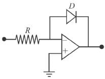
In one of the following circuits, negative feedback does not operate for a negative input. Which one is it ? The Op-Amps are running from supplies.- a)
- b)
- c)
- d)
Correct answer is option 'B'. Can you explain this answer?
In one of the following circuits, negative feedback does not operate for a negative input. Which one is it ? The Op-Amps are running from supplies.
a)
b)
c)
d)
|
|
Jayant Mishra answered |
Since diode does not conduct in reverse bias hence, the circuit given in option (c) does not operate for a negative feedback.
The correct answer is:
The correct answer is:
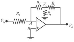
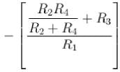
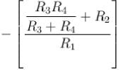
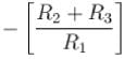
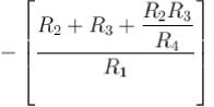
The transistor gain of the circuit shown in figure is given by
- a)
- b)
- c)
- d)
Correct answer is option 'D'. Can you explain this answer?
The transistor gain of the circuit shown in figure is given by
a)
b)
c)
d)
|
|
Vedika Singh answered |
A and B can be measured at the same potential. From figure;
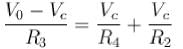

or
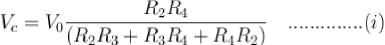
Also
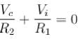
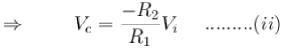
Combing (i) and (ii)
The correct answer is:
or
Also
Combing (i) and (ii)
The correct answer is:
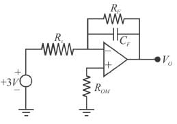
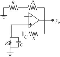
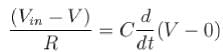
Figure shows a practical integrator with  If a step (dc) voltage of +3V is applied as input for
  ( f in second), the output voltage is.
- a)a ramp function of - 6V
- b)a step function of -12V
- c)a ramp function of - 4V
- d)a ramp function of -1 5V
Correct answer is option 'C'. Can you explain this answer?
Figure shows a practical integrator with If a step (dc) voltage of +3V is applied as input for ( f in second), the output voltage is.
If a step (dc) voltage of +3V is applied as input for ( f in second), the output voltage is.a)
a ramp function of - 6V
b)
a step function of -12V
c)
a ramp function of - 4V
d)
a ramp function of -1 5V
|
|
Vedika Singh answered |
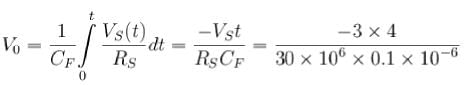
= -4V
The correct answer is: a ramp function of -4V
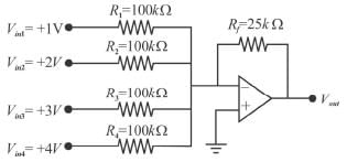
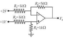
Given the circuit below, calculate the output voltage of the non-inverting Op-Amp summer:
- a)9V
- b)4V
- c)8V
- d)6V
Correct answer is option 'A'. Can you explain this answer?
Given the circuit below, calculate the output voltage of the non-inverting Op-Amp summer:
a)
9V
b)
4V
c)
8V
d)
6V
|
|
Vedika Singh answered |
The output voltage of a non-inverting Op-Amp is.
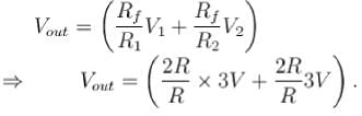
= 9V
The correct answer is: 9V
= 9V
The correct answer is: 9V
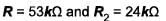
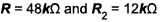
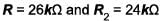
What should be the values of the component R and R2 such the frequency of the Wien bridge oscillator is 300Hz?
(given C = 0.01 μf and R1 = 12kΩ.
- a)
- b)
- c)
- d)
Correct answer is option 'B'. Can you explain this answer?
What should be the values of the component R and R2 such the frequency of the Wien bridge oscillator is 300Hz?
(given C = 0.01 μf and R1 = 12kΩ.
(given C = 0.01 μf and R1 = 12kΩ.
a)
b)
c)
d)
|
|
Pie Academy answered |
The frequency of oscillation f0 is exactly the resonant frequency of balanced Wien bridge and is given by 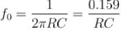
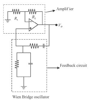
Assuming that the resistor are equal in value, and the capacitors are equal is value in the reactive lag of the wien bridge. At the frequency, the gain required for sustained oscillation is given by
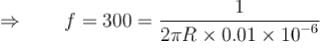
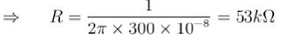
The correct answer is:
Assuming that the resistor are equal in value, and the capacitors are equal is value in the reactive lag of the wien bridge. At the frequency, the gain required for sustained oscillation is given by
The correct answer is:
The natural semiconductor LH0063C has a slew rate of- a)1400V/µs
- b)6000V/µs
- c)500V/µs
- d)None of the mentioned
Correct answer is option 'B'. Can you explain this answer?
The natural semiconductor LH0063C has a slew rate of
a)
1400V/µs
b)
6000V/µs
c)
500V/µs
d)
None of the mentioned
|
|
Ishani Dasgupta answered |
The given information is incomplete. The slew rate of a semiconductor is typically expressed in volts per microsecond (V/μs). Without the complete value, it is not possible to determine the correct answer.
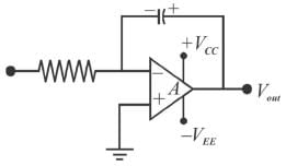
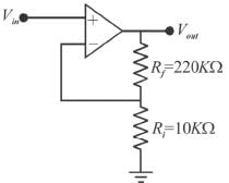
The circuit shown is based on ideal operational amplifiers. It acts as a
- a)subtractor
- b)buffer amplifier
- c)adder
- d)divider
Correct answer is option 'B'. Can you explain this answer?
The circuit shown is based on ideal operational amplifiers. It acts as a
a)
subtractor
b)
buffer amplifier
c)
adder
d)
divider
|
|
Pie Academy answered |
A buffer amplifier (sometimes simply called a buffer) is one that provides electrical impedance transformation from one circuit to another, with the aim of the signal source being unaffected by (“buffered from”) whatever currents that the load may produce.
The correct answer is: buffer amplifier
The correct answer is: buffer amplifier
The certain inverting amplifier has a closed loop gain of 25. The Op-Amp has an open-loop gain of 100000. If another Op-Amp with an open loop gain of 200000 is substituted in the configuration, the closed loop gain is?
Correct answer is '25'. Can you explain this answer?
The certain inverting amplifier has a closed loop gain of 25. The Op-Amp has an open-loop gain of 100000. If another Op-Amp with an open loop gain of 200000 is substituted in the configuration, the closed loop gain is?

|
Hrishikesh Verma answered |
The closed loop gain depends on the configuration and open loop gain is completely independent of it. Hence even if open loop gain is changed, the closed loop gain remains at 25 with the same configuration.
The correct answer is: 25
The correct answer is: 25
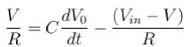
The circuit below represent a non-inverting integrator. Find the expression for the output voltage.
- a)

- b)
- c)
- d)
Correct answer is option 'C'. Can you explain this answer?
The circuit below represent a non-inverting integrator. Find the expression for the output voltage.
a)
b)
c)
d)
|
|
Pie Academy answered |
Let the inverting terminal of Op-Amp is at potential ‘V and hence non-inverting terminal also appears to have the same potential ‘V due to virtual ground concept.
Input current to op-amp is zero. Hence at non-inverting terminal mode, we have
Input current to Op-Amp is zero. Hence at inverting terminal mode we have
Substituting the values and solving all the above equations, we get
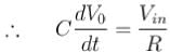
The circuit connection of Op-Amp given in the figure (i) and (ii) represent
- a)Detectors for figure (i) and logarithmic amplifier for figure (ii)
- b)Logarithmic amplifier for figure (i) and detector for figure (ii)
- c)Logarithmic amplifier for both figure (i) and (ii)
- d)Detectors for both figure (i) and (iii)
Correct answer is option 'B'. Can you explain this answer?
The circuit connection of Op-Amp given in the figure (i) and (ii) represent
a)
Detectors for figure (i) and logarithmic amplifier for figure (ii)
b)
Logarithmic amplifier for figure (i) and detector for figure (ii)
c)
Logarithmic amplifier for both figure (i) and (ii)
d)
Detectors for both figure (i) and (iii)
|
|
Jayant Mishra answered |
The circuit connection of Op-Amp given in figure (i) and (ii) represents logarithmic amplifier for figure (i) and detector for figure (ii)
The correct answer is: Logarithmic amplifier for figure (i) and detector for figure (ii)
The correct answer is: Logarithmic amplifier for figure (i) and detector for figure (ii)
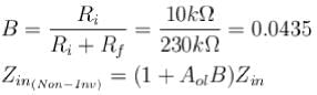
The data of Op-Amp shown in figure is.
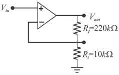
Zin = 2MΩ, ZOut = 75Ω and AoI = 200000, then the correct matching pairs is.- a)Input impedance = +17.4GΩ
- b)Output impedance = +28.6MΩ
- c)Close loop voltage gain = +125.0
- d)Attenuation of the feedback = +0.0435
Correct answer is option 'A,D'. Can you explain this answer?
The data of Op-Amp shown in figure is.
Zin = 2MΩ, ZOut = 75Ω and AoI = 200000, then the correct matching pairs is.
Zin = 2MΩ, ZOut = 75Ω and AoI = 200000, then the correct matching pairs is.
a)
Input impedance = +17.4GΩ
b)
Output impedance = +28.6MΩ
c)
Close loop voltage gain = +125.0
d)
Attenuation of the feedback = +0.0435
|
|
Pie Academy answered |
The attenuation, B, of the feedback circuit is
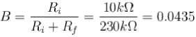
= [1 + (200000)(0.0435)](2MΩ)
= 17.4 GΩ
= 8.6mΩ
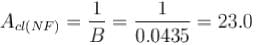
The correct answers are: Attenuation of the feedback = +0.0435, Input impedance = +17.4 GΩ
= [1 + (200000)(0.0435)](2MΩ)
= 17.4 GΩ
= 8.6mΩ
The correct answers are: Attenuation of the feedback = +0.0435, Input impedance = +17.4 GΩ
How many PN junctions is/are present in a bipolar junction transistor?
Correct answer is '2'. Can you explain this answer?
How many PN junctions is/are present in a bipolar junction transistor?
|
|
Jay Nambiar answered |
Introduction:
A bipolar junction transistor (BJT) is a three-layer semiconductor device that consists of two PN junctions. It is widely used in electronic circuits for amplification, switching, and signal processing. Understanding the number of PN junctions in a BJT is crucial for analyzing its behavior and characteristics.
Explanation:
A BJT is composed of three semiconductor regions, namely the emitter, base, and collector. Each region is doped differently to create the necessary PN junctions. Let's examine the PN junctions in a BJT in detail:
1. Emitter-Base Junction:
The emitter-base junction is formed between the heavily doped emitter region and the lightly doped base region. This junction is a PN junction, where the P-region is the base and the N-region is the emitter. The emitter-base junction is forward-biased to allow the flow of majority carriers (electrons in an NPN transistor) from the emitter to the base.
2. Base-Collector Junction:
The base-collector junction is formed between the lightly doped base region and the moderately doped collector region. This junction is also a PN junction, where the P-region is the base and the N-region is the collector. The base-collector junction is reverse-biased to prevent the majority carriers (electrons) injected from the emitter from flowing into the collector.
Summary:
In a bipolar junction transistor, there are two PN junctions:
1. Emitter-Base Junction
2. Base-Collector Junction
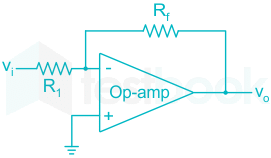
The inverting input terminal of an operational amplifier (Op-Amp) is shorted with output terminal apart from being grounded. A voltage signal V1 is applied to the noninverting input terminal of the Op-Amp. Under this configuration the Op-Amp function is as :- a)voltage to current converter
- b)an oscillator
- c)an open loop inverter
- d)a voltage follower
Correct answer is option 'D'. Can you explain this answer?
The inverting input terminal of an operational amplifier (Op-Amp) is shorted with output terminal apart from being grounded. A voltage signal V1 is applied to the noninverting input terminal of the Op-Amp. Under this configuration the Op-Amp function is as :
a)
voltage to current converter
b)
an oscillator
c)
an open loop inverter
d)
a voltage follower
|
|
Jayant Mishra answered |
The lowest gain can be obtained from a non-inverting amplifier with feedback 1.
When the non-inverting amplifier is configured for unit gain, it is called a voltage follower because the output voltage is equal to and in phase with the input. In other words, in the voltage follower, the output follows the input. To obtain the voltage follower from non-inverting amplifier of figure 1. simply open R1 and short R
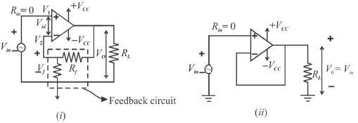
The correct answer is: a voltage follower
When the non-inverting amplifier is configured for unit gain, it is called a voltage follower because the output voltage is equal to and in phase with the input. In other words, in the voltage follower, the output follows the input. To obtain the voltage follower from non-inverting amplifier of figure 1. simply open R1 and short R
f
The resulting circuit is shown is figure 2. In this figure, all the output voltages are feedback into the inverting terminal of the Op-Amp ; consequently the gain of the feedback is 1.The correct answer is: a voltage follower
The midrange open-loop gain of an Op-Amp :- a)extends from the lower critical frequency to the upper critical frequency
- b)extends from 0Hz to the upper critical frequency
- c)rolls off at 20 dB/decade beginning at 0Hz
- d)both (b) and (c)
Correct answer is option 'B'. Can you explain this answer?
The midrange open-loop gain of an Op-Amp :
a)
extends from the lower critical frequency to the upper critical frequency
b)
extends from 0Hz to the upper critical frequency
c)
rolls off at 20 dB/decade beginning at 0Hz
d)
both (b) and (c)
|
|
Jayant Mishra answered |
It extends from 0Hz to the upper critical frequency.
The correct answer is: extends from 0Hz to the upper critical frequency
The correct answer is: extends from 0Hz to the upper critical frequency
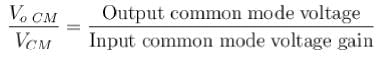
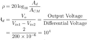
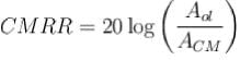
The Common Mode Rejection Ratio (CMRR) of a differential amplifier using an operational amplifier is 100 dB. The output voltage for a differential input of is 2V. The common mode gain is (in dB)
Correct answer is '0.1'. Can you explain this answer?
The Common Mode Rejection Ratio (CMRR) of a differential amplifier using an operational amplifier is 100 dB. The output voltage for a differential input of is 2V. The common mode gain is (in dB)
|
|
Niti Mukherjee answered |
Where Ad = differential voltage gain
= large signal voltage gains
= Common mode voltage gain
The CMRR is generally expressed is dB and denoted by
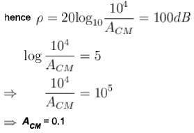
The correct answer is: 0.1
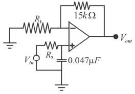
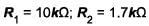
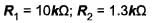
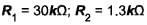
The low-pass active filter shown in the figure has a cut-off frequency of 2kHz and a pass band gain of 1.5. The values of the resistors are :
- a)
- b)
- c)
- d)

Correct answer is option 'D'. Can you explain this answer?
The low-pass active filter shown in the figure has a cut-off frequency of 2kHz and a pass band gain of 1.5. The values of the resistors are :
a)
b)
c)
d)
|
|
Pie Academy answered |
At f = fcc (cut o ff frequency at which gain falls to  of its low frequency value)
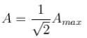
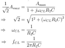
(i) Pass-Band gain = Amax = 1.5.
Hence,
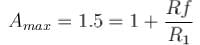
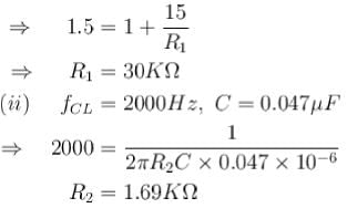
The correct answer is: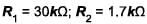
of its low frequency value)(i) Pass-Band gain = Amax = 1.5.
Hence,
The correct answer is:
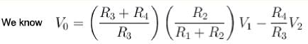
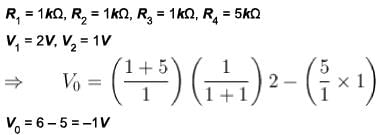
The output V02 (at the end of third Op-Amp) of the below circuit is :
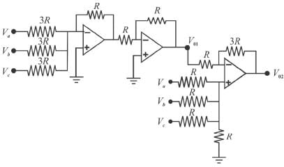
- a)
- b)
- c)
- d)

Correct answer is option 'B'. Can you explain this answer?
The output V02 (at the end of third Op-Amp) of the below circuit is :
a)
b)
c)
d)
|
|
Pie Academy answered |
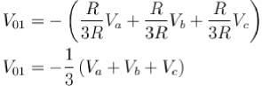
Similarly
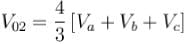
The correct answer is:
If a certain Op-Amp has a mid range open-loop gain of 200000 and a unity-gain frequency of 5MHz, the gain bandwidth product in Hz is :
Correct answer is '5000000'. Can you explain this answer?
If a certain Op-Amp has a mid range open-loop gain of 200000 and a unity-gain frequency of 5MHz, the gain bandwidth product in Hz is :
|
|
Saanvi Roy answered |
gain bandwidth product = frequency at which gain is unity
= 5 MHz
= 5000000 Hz
The correct answer is: 5000000
= 5 MHz
= 5000000 Hz
The correct answer is: 5000000
The Op-Amp has the following parameters; Aol = 50000; Zin = 4MΩ and Zout = 50Ω. The values of input impedance, output impedance and close loop voltage gains are :
- a)

- b)

- c)

- d)

Correct answer is option 'A,C'. Can you explain this answer?
The Op-Amp has the following parameters; Aol = 50000; Zin = 4MΩ and Zout = 50Ω. The values of input impedance, output impedance and close loop voltage gains are :
a)
b)
c)
d)
|
|
Vedika Singh answered |
The feedback attenuation B is
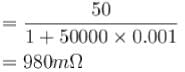
zero for all practical purposes. The closed loop voltage gain is.
The correct answers are: Zout = 980mΩ, Acl(t) = -100
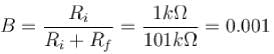
Common-mode rejection ratio is given by- a)
- b)
- c)

- d)
Correct answer is option 'A,B'. Can you explain this answer?
Common-mode rejection ratio is given by
a)
b)
c)
d)
|
|
Jayant Mishra answered |
The correct answers are:
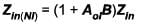
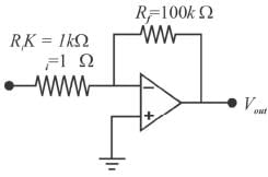
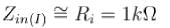
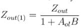
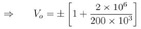
The input and output impedance of the amplifier in given figure, is, (The Op-amp data sheet gives Zin = 2MΩ, ZOut = 75Ω and Aol = 200000).
- a)17.4GΩ; 8.6mΩ
- b)8.6GGΩ; 17.4mΩ
- c)7.4GΩ; 3.6mΩ
- d)7.4GΩ; 8.6mΩ
Correct answer is option 'A'. Can you explain this answer?
The input and output impedance of the amplifier in given figure, is, (The Op-amp data sheet gives Zin = 2MΩ, ZOut = 75Ω and Aol = 200000).
a)
17.4GΩ; 8.6mΩ
b)
8.6GGΩ; 17.4mΩ
c)
7.4GΩ; 3.6mΩ
d)
7.4GΩ; 8.6mΩ
|
|
Pie Academy answered |
The attenuation B, of the feedback circuit is
= [1 + 200000(0.0435)](2MΩ)
= 17.4GΩ
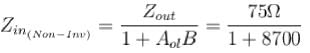
= 8.6Ω
The correct answer is: 17.4GΩ; 8.6/mΩ
= [1 + 200000(0.0435)](2MΩ)
= 17.4GΩ
= 8.6Ω
The correct answer is: 17.4GΩ; 8.6/mΩ
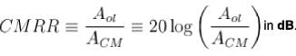
A certain Op-Amp has an open loop voltage gain of 1,00,000 and a common mode gain of 0.2. The CMRR is :- a)500000
- b)114 dB
- c)22.8 dB
- d)100000
Correct answer is option 'A,B'. Can you explain this answer?
A certain Op-Amp has an open loop voltage gain of 1,00,000 and a common mode gain of 0.2. The CMRR is :
a)
500000
b)
114 dB
c)
22.8 dB
d)
100000
|
|
Jayant Mishra answered |
Aol = 100000
Acm = 0.2
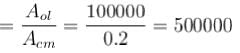
Expressed in decibels
CMRR =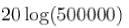
= 114dB
The correct answers are: 500000, 114 dB
Acm = 0.2
Expressed in decibels
CMRR =
= 114dB
The correct answers are: 500000, 114 dB
In order to obtain a solution of the differential equation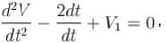
involving voltage V(t) and V1 an Op-Amp circuit would require at least.- a)one Op-Amp adder
- b)two Op-Amp adder
- c)one Op-Amp integrator
- d)two Op-Amp integrator
Correct answer is option 'A,D'. Can you explain this answer?
In order to obtain a solution of the differential equation
involving voltage V(t) and V1 an Op-Amp circuit would require at least.
involving voltage V(t) and V1 an Op-Amp circuit would require at least.
a)
one Op-Amp adder
b)
two Op-Amp adder
c)
one Op-Amp integrator
d)
two Op-Amp integrator
|
|
Jayant Mishra answered |
Since, it is a two degree linear differential equation, hence, two integrators are required, also one adder to calculate the sum of outputs.
The correct answers are: two Op-Amp integrator , one Op-Amp adder
The correct answers are: two Op-Amp integrator , one Op-Amp adder
The frequency at which the open loop gain is equal to 1 is called. - a)The upper critical frequency
- b)The notch frequency
- c)The cut-off frequency
- d)The unity-gain frequency
Correct answer is option 'D'. Can you explain this answer?
The frequency at which the open loop gain is equal to 1 is called.
a)
The upper critical frequency
b)
The notch frequency
c)
The cut-off frequency
d)
The unity-gain frequency
|
|
Jayant Mishra answered |
It is called the unity-gain frequency
The correct answer is: The unity-gain frequency
The correct answer is: The unity-gain frequency
The gain of the amplifier shown in figure. The open loop voltage gain of the Op-Amp is 1,00,000.
This is a non-inverting Op-Amp configuration. Therefore, the closed loop voltage gain is
Correct answer is '22.3'. Can you explain this answer?
The gain of the amplifier shown in figure. The open loop voltage gain of the Op-Amp is 1,00,000.
This is a non-inverting Op-Amp configuration. Therefore, the closed loop voltage gain is
This is a non-inverting Op-Amp configuration. Therefore, the closed loop voltage gain is
|
|
Akanksha Choudhary answered |
This is a non-inverting Op-Amp configuration. Therefore, the closed loop voltage gain is
= 22.3
The correct answer is: 22.3
If a certain Op-Amp has a closed loop gain of 20 and an upper critical frequency of 10 MHz, the gain bandwidth product is :- a)50 MHz
- b)200 MHz
- c)10 MHz
- d)40 MHz
Correct answer is option 'B'. Can you explain this answer?
If a certain Op-Amp has a closed loop gain of 20 and an upper critical frequency of 10 MHz, the gain bandwidth product is :
a)
50 MHz
b)
200 MHz
c)
10 MHz
d)
40 MHz
|
|
Pie Academy answered |
To determine the gain bandwidth product of an op-amp:
- The closed-loop gain is 20.
- The upper critical frequency is 10 MHz.
Using the relationship:
- Gain-bandwidth product = Closed-loop gain x Upper critical frequency
Thus, the calculation becomes:
- Gain-bandwidth product = 20 x 10 MHz = 200 MHz
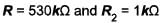
Figure shows a practical integrator with Rs = 30MΩ, RF = 20MΩ and CF = 0.1 μF. If a step (dc) voltage of +3V is applied as input for 0 < t < 4 (t is in seconds), the output voltage is a ramp function. What is the voltage in volts?
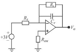
Correct answer is '-4'. Can you explain this answer?
Figure shows a practical integrator with Rs = 30MΩ, RF = 20MΩ and CF = 0.1 μF. If a step (dc) voltage of +3V is applied as input for 0 < t < 4 (t is in seconds), the output voltage is a ramp function. What is the voltage in volts?
|
|
Tarun Singh answered |
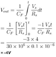
The correct answer is: -4
The circuit shown below represent a non-inverting integrator. For high frequency input (ω →  ) impedance in ohms is?
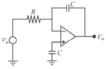
Correct answer is '0'. Can you explain this answer?
The circuit shown below represent a non-inverting integrator. For high frequency input (ω → ) impedance in ohms is?
) impedance in ohms is?|
|
Athul Chaudhary answered |
Input impedance is given as 
For (ω → ) input impedance → 0
The correct answer is: 0
For (ω →
) input impedance → 0The correct answer is: 0
A bistable multi vibrator with a saturation voltage 15Vis shown in the diagram. The magnitude of the positive and negative thresholds at the inverting terminal for which the multi vibrator will switch to the other state are in volts (up to 2 decimal places).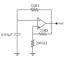
Correct answer is '0.45'. Can you explain this answer?
A bistable multi vibrator with a saturation voltage 15Vis shown in the diagram. The magnitude of the positive and negative thresholds at the inverting terminal for which the multi vibrator will switch to the other state are in volts (up to 2 decimal places).
|
|
Swara Reddy answered |
The threshold voltage is 
where
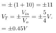
The correct answer is: 0.45
where
The correct answer is: 0.45
The output Vo of the ideal Op-Amp circuit shown is the figure is (in volts).
Correct answer is '-7'. Can you explain this answer?
The output Vo of the ideal Op-Amp circuit shown is the figure is (in volts).
|
|
Shreya Chauhan answered |
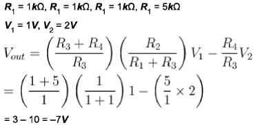
The correct answer is: -7
In the given circuit using ideal Op-Amps, the output voltage (in mV) is :
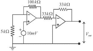
Correct answer is '-200'. Can you explain this answer?
In the given circuit using ideal Op-Amps, the output voltage (in mV) is :
|
|
Partho Gupta answered |
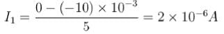
Hence, V1= 2x106 x100x103 = 200x10-3V
Since, gain of second stage is -1
⇒ Vout = - 200mV
The correct answer is: -200
An averaging amplifier has five inputs. Ratio  must be?
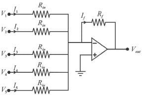
Correct answer is '0.2'. Can you explain this answer?
An averaging amplifier has five inputs. Ratio must be?
must be?|
|
Nilotpal Basu answered |
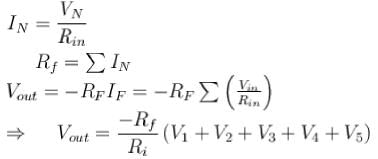
Now to average 5 inputs, Rf should be

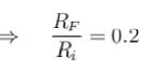
The correct answer is: 0.2
Chapter doubts & questions for Operational Amplifier - Electronics for GATE 2025 is part of GATE Physics exam preparation. The chapters have been prepared according to the GATE Physics exam syllabus. The Chapter doubts & questions, notes, tests & MCQs are made for GATE Physics 2025 Exam. Find important definitions, questions, notes, meanings, examples, exercises, MCQs and online tests here.
Chapter doubts & questions of Operational Amplifier - Electronics for GATE in English & Hindi are available as part of GATE Physics exam.
Download more important topics, notes, lectures and mock test series for GATE Physics Exam by signing up for free.
Electronics for GATE
55 videos|28 docs|20 tests
|
|
© EduRev
|
Education Revolution
|


|


Signup on EduRev and stay on top of your study goals
10M+ students crushing their study goals daily