


All Exams >
Electrical Engineering (EE) >
Analog and Digital Electronics >
All Questions
All questions of A/D & D/A Converters and Sample/Hold Circuits for Electrical Engineering (EE) Exam
Increase the order of data hold will- a)improve the stability of the system
- b)decrease the time delay
- c)increase the time delay
- d)increase the time constant
Correct answer is option 'C'. Can you explain this answer?
Increase the order of data hold will
a)
improve the stability of the system
b)
decrease the time delay
c)
increase the time delay
d)
increase the time constant

|
EduRev GATE answered |
Data Hold
Data hold is a process of generating a continuous-time signal h(t) from a discrete-time sequence x(kT).
The signal h(t) during the time interval kT ≤ t ≤ (k + 1)T may be approximated by a polynomial in τ as follows:
h(kT + τ ) = anτn + an−1τn−1 + ··· + a1τ + a0
Where 0 ≤ τ ≤ T
Data hold is a process of generating a continuous-time signal h(t) from a discrete-time sequence x(kT).
The signal h(t) during the time interval kT ≤ t ≤ (k + 1)T may be approximated by a polynomial in τ as follows:
h(kT + τ ) = anτn + an−1τn−1 + ··· + a1τ + a0
Where 0 ≤ τ ≤ T
Note: h(kT) = x(kT)
h(kT + τ ) = anτn + an−1τn−1 + ··· + a1τ + x(kT)
If the data hold circuit is an nth-order polynomial extrapolator, it is called an nth-order hold. It uses the past n + 1 discrete data x((k − n)T), x((k − n + 1)T), ··· , x(kT) to generate h(kT + τ ).
h(kT + τ ) = anτn + an−1τn−1 + ··· + a1τ + x(kT)
If the data hold circuit is an nth-order polynomial extrapolator, it is called an nth-order hold. It uses the past n + 1 discrete data x((k − n)T), x((k − n + 1)T), ··· , x(kT) to generate h(kT + τ ).
Conclusion:
As the order of the data hold increases the circuit order(n) also increases which leads to the further increase in the time delay because it has to use past n + 1 samples.
Option 3 is correct.
As the order of the data hold increases the circuit order(n) also increases which leads to the further increase in the time delay because it has to use past n + 1 samples.
Option 3 is correct.

The fastest type of Analog to Digital converter is- a)Counter type
- b)Tracking type
- c)Successive approximation type
- d)Parallel comparator type
Correct answer is option 'D'. Can you explain this answer?
The fastest type of Analog to Digital converter is
a)
Counter type
b)
Tracking type
c)
Successive approximation type
d)
Parallel comparator type
|
|
Lakshmi Desai answered |
Understanding Analog to Digital Converters (ADCs)
Analog to Digital Converters (ADCs) are essential components in electronic systems, converting continuous analog signals into discrete digital values. The speed of an ADC is critical in applications requiring rapid signal processing.
Types of ADCs
- Counter type: This type of ADC counts pulses until it reaches the value of the input voltage. It is relatively slow due to the time taken to count each pulse.
- Tracking type: Also known as a sample-and-hold ADC, it tracks the input signal and converts it. While faster than the counter type, it still lags behind in speed compared to other methods.
- Successive approximation type: This method uses a binary search algorithm to converge on the input signal's value. It is faster than the counter and tracking types but still not the fastest.
- Parallel comparator type: This ADC uses multiple comparators to compare the input voltage directly against reference voltages simultaneously. This parallel processing allows it to achieve very high speeds, making it the fastest among the listed types.
Why Parallel Comparator is the Fastest
- Simultaneous comparisons: By evaluating several reference voltages at once, it minimizes the time taken for conversion.
- High throughput: Capable of processing multiple bits in a single clock cycle, thus increasing overall data rate.
- Applications: Ideal for high-speed applications such as digital oscilloscopes, video processing, and telecommunications, where rapid signal conversion is crucial.
In summary, the parallel comparator type ADC is the fastest due to its ability to perform multiple comparisons at once, leading to shorter conversion times compared to other types. This efficiency is vital in high-speed electronic applications.
The analog-to-digital converters are employed in: - a)Voltmeter
- b)Wattmeter
- c)Energy meter
- d)Digital multimeter
Correct answer is option 'D'. Can you explain this answer?
The analog-to-digital converters are employed in:
a)
Voltmeter
b)
Wattmeter
c)
Energy meter
d)
Digital multimeter
|
|
Kajal Yadav answered |
Understanding Analog-to-Digital Converters (ADCs)
Analog-to-Digital Converters (ADCs) are essential components in electronic measurement systems that convert analog signals into digital data. This conversion allows for easier processing, storage, and analysis of information.
Role of ADCs in Measurement Devices
- Voltmeter: Traditional voltmeters can be analog or digital. While digital voltmeters use ADCs, analog voltmeters do not require them as they display voltage values on a scale.
- Wattmeter: Wattmeters measure electrical power but can be either analog or digital. Analog wattmeters operate without ADCs, while digital models do use them for displaying values.
- Energy Meter: Similar to wattmeters, energy meters can also be analog or digital. Analog energy meters directly measure and display energy without the need for conversion, while digital versions use ADCs.
Why Digital Multimeter (DMM) Uses ADCs
- Digital Multimeter (DMM): DMMs are versatile instruments that measure voltage, current, and resistance. They require precise conversion of analog signals to digital for accurate readings.
- Measurement Accuracy: ADCs in DMMs enable higher accuracy and reliability in measurements. The digital output can be processed, stored, and analyzed easily.
- User Interface: The digital format of measurements in DMMs allows for clear and easy interpretation of data, often with additional features like auto-ranging and data logging.
In summary, while other devices may incorporate both analog and digital types, ADCs are specifically critical for the functioning of digital multimeters, making option 'D' the correct choice.
Two 10-bit ADCs, one of successive approximation type and other of single slope integrating type, take Ta and Tb time respectively to convert 3V analog input signal to digital output. If the input analog signal is increased to 6V, the approximate time taken by the two ADCs will respectively be- a)2Ta, 2Tb
- b)Ta, Tb
- c)Ta, 2Tb
- d)2Ta, Tb
Correct answer is option 'D'. Can you explain this answer?
Two 10-bit ADCs, one of successive approximation type and other of single slope integrating type, take Ta and Tb time respectively to convert 3V analog input signal to digital output. If the input analog signal is increased to 6V, the approximate time taken by the two ADCs will respectively be
a)
2Ta, 2Tb
b)
Ta, Tb
c)
Ta, 2Tb
d)
2Ta, Tb

|
Gate Funda answered |
- For the successive approximation ADC, the conversion time is proportional to the input voltage range, so for a 6V input signal, the conversion time will be 2 times Ta. Therefore, the approximate time taken by the successive approximation ADC for a 6V input signal will be 2Ta.
- For the single slope integrating ADC, the conversion time is also proportional to the input voltage range, so for a 6V input signal, the conversion time will be 2 times Tb. Therefore, the approximate time taken by the single slope integrating ADC for a 6V input signal will be Tb.
- Therefore, the approximate time taken by the two ADCs for a 6V input signal will be 2Ta for the successive approximation ADC and Tb for the single slope integrating ADC.
The resolution of a dual slope ADC can be increased by- a)Increasing the reference voltage magnitude
- b)Improving the reference voltage accuracy
- c)Increasing the clock frequency
- d)Increasing the clock stability
Correct answer is option 'C'. Can you explain this answer?
The resolution of a dual slope ADC can be increased by
a)
Increasing the reference voltage magnitude
b)
Improving the reference voltage accuracy
c)
Increasing the clock frequency
d)
Increasing the clock stability
|
|
EduRev GATE answered |
The resolution of the dual-slope ADC is determined by the length of the run-down period and by the time measurement resolution (i.e., the frequency of the controller's clock).
The resolution (in the number of bits) is the minimum length of the run-down period for a full-scale input(Vin = - Vref).

Where td is the run-down period,
r is resolution
fclk is the frequency of the clock.
The resolution (in the number of bits) is the minimum length of the run-down period for a full-scale input(Vin = - Vref).
Where td is the run-down period,
r is resolution
fclk is the frequency of the clock.
Important Point:
There are limits to the maximum resolution of the dual-slope integrating ADC. It is not possible to increase the resolution of the basic dual-slope ADC to arbitrarily high values by using longer measurement times or faster clocks.
Among the following four, the slowest ADC (analog-to-digital converter) is- a)Parallel-comparator (flash) type
- b)Successive approximation type
- c)Integrating type
- d)Counting type
Correct answer is option 'C'. Can you explain this answer?
Among the following four, the slowest ADC (analog-to-digital converter) is
a)
Parallel-comparator (flash) type
b)
Successive approximation type
c)
Integrating type
d)
Counting type
|
|
Gate Funda answered |
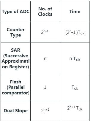
Integrating type ADC is the slowest.
The conversion time of different ADC is shown below.
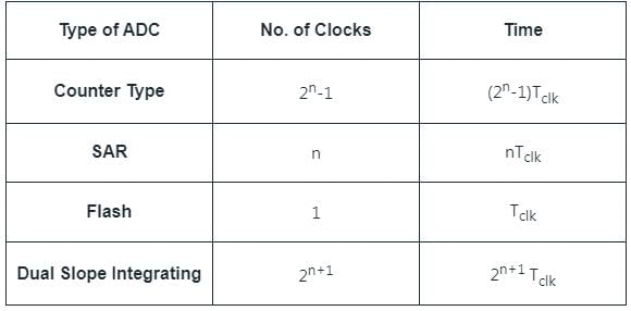
From the above table, the fastest ADC is Flash Type ADC whose conversion time is independent of the number of bits.
From the above table, the fastest ADC is Flash Type ADC whose conversion time is independent of the number of bits.
Which of the following is NOT an Analog-to-Digital Converter? - a)Successive Approximation Converter
- b)Counter Type
- c)Dual Slope Converter
- d)R-2R Ladder
Correct answer is option 'D'. Can you explain this answer?
Which of the following is NOT an Analog-to-Digital Converter?
a)
Successive Approximation Converter
b)
Counter Type
c)
Dual Slope Converter
d)
R-2R Ladder
|
|
Gate Funda answered |
Concept:
The common Analog to digital converters are:
Ramp-type:
- The principle of Ramp-type DVM is based on the measurement of the time it takes for a linear ramp voltage to rise from 0 V to the level of the input voltage (or) to decrease from the level of the input voltage to zero.
- This type of Analogue to Digital Converter is very slow (but cheap and simple).
- It is ideal for data that changes fairly slowly such as vehicle or aircraft control systems.
- Audio signals are slow enough to be converted.
Dual-slope converter:
- In the dual-slope technique, an integrator is used to integrate an accurate voltage reference for a fixed period of time. The same integrator is then used to integrate with the reverse slope, the input voltage, and the time required to return to the starting voltage is measured.
- The automatic zero correction function is performed before each conversion so that changes in the offset voltages & current will be compensated.
Successive Approximation:
- The basic principle is binary regression, in which analog input is compared with DAC reference voltage which is repeatedly divided in half.
- A successive approximation A/D converter consists of a comparator, a successive approximation register (SAR), output latches, and a D/A converter.
- It is capable of high speed and is reliable.
Important Points
R-2R ladder is used for Digital to Analog Converter:
It uses a summing amplifier with an R-2R ladder network as shown below.
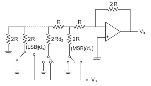
For n-bit DAC, it requires only 2 different values of resistors i.e. R and 2R.
It uses a summing amplifier with an R-2R ladder network as shown below.
For n-bit DAC, it requires only 2 different values of resistors i.e. R and 2R.
The number of comparator circuits required to build a three - bit simultaneous A/D convertor is:- a)15
- b)7
- c)8
- d)16
Correct answer is option 'B'. Can you explain this answer?
The number of comparator circuits required to build a three - bit simultaneous A/D convertor is:
a)
15
b)
7
c)
8
d)
16

|
Telecom Tuners answered |
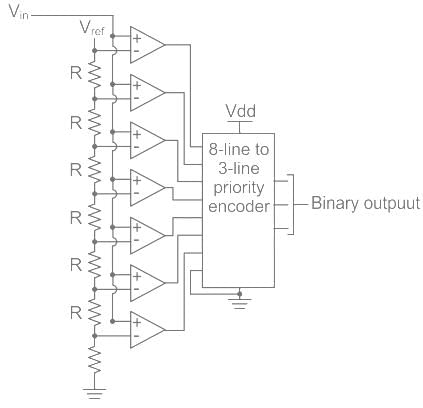
Flash type (or) Parallel type (or) Simultaneous ADC:
The following figure shows a 3-bit flash ADC circuit.
The following figure shows a 3-bit flash ADC circuit.
- It is formed of a series of comparators, each one comparing the input signal to a unique reference voltage.
- The comparator outputs connect to the inputs of a priority encoder circuit, which then produces a binary output.
- Vref is a stable reference voltage provided by a precision voltage regulator as part of the converter circuit.
- As the analog input voltage exceeds the reference voltage at each comparator, the comparator outputs will sequentially saturate to a high state.
- The priority encoder generates a binary number based on the highest-order active input, ignoring all other active inputs.
- Flash type ADC is fastest ADC
- Flash type ADC requires no counter
- For an n-bit ADC, flash type ADC requires (2n – 1) comparators
- Conversion time: Tclk
Calculation:
Given that, n = 3
Number of required comparators, N = 23 – 1 = 7
Given that, n = 3
Number of required comparators, N = 23 – 1 = 7
Given below are three types of converters - successive approximation type
- weighted resistor type
- R-2R ladder type
Which one of the types are D to A converter? - a)only 1 and 2
- b)only 2 and 3
- c)only 1 and 3
- d)1, 2 and 3
Correct answer is option 'B'. Can you explain this answer?
Given below are three types of converters
- successive approximation type
- weighted resistor type
- R-2R ladder type
Which one of the types are D to A converter?
a)
only 1 and 2
b)
only 2 and 3
c)
only 1 and 3
d)
1, 2 and 3
|
|
Ishan Chawla answered |
Understanding D to A Converters
In the context of Digital to Analog (D to A) converters, it's essential to identify which types among the listed options are indeed D to A converters.
Types of Converters
1. Successive Approximation Type
- This converter uses a binary search approach to convert digital signals into analog signals.
- It is efficient and widely used in applications requiring moderate speeds and precision.
2. Weighted Resistor Type
- This type utilizes a set of resistors with different weights corresponding to binary values.
- It combines the contributions of each resistor to produce the final analog output.
- It is a fundamental D to A converter design.
3. R-2R Ladder Type
- This design uses a repetitive structure of resistors in a ladder configuration.
- It simplifies the process of creating weighted outputs and is known for its accuracy in producing an analog signal from a digital input.
Correct Answer Analysis
The question asked which of the types are D to A converters. Here’s the breakdown:
- Successive Approximation Type: D to A converter.
- Weighted Resistor Type: D to A converter.
- R-2R Ladder Type: D to A converter.
Conclusion
In conclusion, all three types can function as D to A converters. However, the correct answer provided (option 'B' – only 2 and 3) is incorrect if we consider all three types as capable D to A converters. The correct understanding is that:
- All three types are valid D to A converters.
Thus, the correct answer should be option 'D', which includes all three types.
What is the SNR of an ideal 10 bit ADC ?- a)81.96 dB
- b)51.96 dB
- c)61.96 dB
- d)71.96 dB
Correct answer is option 'C'. Can you explain this answer?
What is the SNR of an ideal 10 bit ADC ?
a)
81.96 dB
b)
51.96 dB
c)
61.96 dB
d)
71.96 dB
|
|
EduRev GATE answered |
Concept:
- SNR (Signal-to-Noise Ratio) of an ADC (Analog-to-Digital Converter) is a measure of the quality of the ADC's output signal.
- It represents the ratio of the amplitude of the input signal to the amplitude of the noise present in the output signal. In other words, it is a measure of how much the signal level exceeds the noise level in the output of the ADC.
- SNR is a calculated value that represents the ratio of RMS signal to RMS noise.
- If we multiply the log10 of this ratio by 20 to derive SNR in decibels.
- An ADC’s ideal SNR equals 6.02N + 1.76 dB, where N is the number of bits.
Calculation:
SNR of an 10 bit ADC = 6.02 × 10 + 1.76 =61.96 dB
Hence the correct answer is option 3.
SNR of an 10 bit ADC = 6.02 × 10 + 1.76 =61.96 dB
Hence the correct answer is option 3.
How many comparators are used in a 4-bit flash Analog-to-Digital Converter (ADC)?- a)4
- b)5
- c)15
- d)16
Correct answer is option 'C'. Can you explain this answer?
How many comparators are used in a 4-bit flash Analog-to-Digital Converter (ADC)?
a)
4
b)
5
c)
15
d)
16
|
|
Telecom Tuners answered |
Concept:
Flash Type ADC:
1) It is the fastest ADC among all the ADC types.
2) An n-bit flash type ADC requires: 2n -1 comparators, 2n resistors, and one 2n × n priority encoder.
Analysis: Number of bits(n) = 4
Number of comparators required = 24 -1 = 15
Flash Type ADC:
1) It is the fastest ADC among all the ADC types.
2) An n-bit flash type ADC requires: 2n -1 comparators, 2n resistors, and one 2n × n priority encoder.
Analysis: Number of bits(n) = 4
Number of comparators required = 24 -1 = 15
A 5 bit ladder has a digital input of 11010. Assuming that 0 corresponds to 0 V and 1 corresponds to +10 V, its output voltage will be:- a)+ 6.5 V
- b)– 6.5 V
- c)– 8.125 V
- d)+ 8.125 V
Correct answer is option 'D'. Can you explain this answer?
A 5 bit ladder has a digital input of 11010. Assuming that 0 corresponds to 0 V and 1 corresponds to +10 V, its output voltage will be:
a)
+ 6.5 V
b)
– 6.5 V
c)
– 8.125 V
d)
+ 8.125 V
|
|
Gate Funda answered |
Concept:
For a ladder-type D/A Converter:
Output Voltage (V0) = Resolution × Decimal Equivalent of binary input.
Where Resolution is given by:
For a ladder-type D/A Converter:
Output Voltage (V0) = Resolution × Decimal Equivalent of binary input.
Where Resolution is given by:
Application:
Given n = 5 and the Digital input = 11010
∵ The Resolution will be:
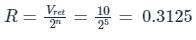
Since the decimal Equivalent of 11010 = 26
So, V0 = 26 × 0.3125
V0 = 8.125 V
Note: If the full-scale voltage is given, then:
Given n = 5 and the Digital input = 11010
∵ The Resolution will be:
Since the decimal Equivalent of 11010 = 26
So, V0 = 26 × 0.3125
V0 = 8.125 V
Note: If the full-scale voltage is given, then:
Which of the following is the fastest A-D converter?- a)Successive approximation type
- b)Flash type
- c)Integration type
- d)Ramp type
Correct answer is option 'B'. Can you explain this answer?
Which of the following is the fastest A-D converter?
a)
Successive approximation type
b)
Flash type
c)
Integration type
d)
Ramp type
|
|
EduRev GATE answered |
Concept:
Flash ADC (Fastest)
- The flash ADC is the fastest type available. A flash ADC uses comparators, one per voltage step, and a string of resistors.
- Flash-type ADC requires no counter For an n-bit ADC, flash-type ADC requires (2n – 1) comparators
- A 4-bit ADC will have 15 comparators, and an 8-bit ADC will have 255 comparators.
- The following figure shows a 3-bit flash ADC circuit.
- It is formed of a series of comparators, each one comparing the input signal to a unique reference voltage.
- The comparator outputs connect to the inputs of a priority encoder circuit, which then produces a binary output.
- Vref is a stable reference voltage provided by a precision voltage regulator as part of the converter circuit.
- As the analog input voltage exceeds the reference voltage at each comparator, the comparator outputs will sequentially saturate to a high state.
- The priority encoder generates a binary number based on the highest-order active input, ignoring all other active inputs.
Additional Information
- The successive approximation A/D converter has a shorter conversion time compared to the counter ramp A/D converter.
- Counter type ADC and successive approximate ADC use DAC Counter type ADC uses linear search and successive approximation type ADC uses binary search
- A ring counter is used in successive approximation-type ADC
- Dual slope ADC is the most accurate
If the resolution of a digital-to-analog converter is approximately 0.4% of its full-scale range, then it is a/an _______.- a)16-bit converter
- b)10-bit converter
- c)8-bit converter
- d)12-bit converter
Correct answer is option 'C'. Can you explain this answer?
If the resolution of a digital-to-analog converter is approximately 0.4% of its full-scale range, then it is a/an _______.
a)
16-bit converter
b)
10-bit converter
c)
8-bit converter
d)
12-bit converter
|
|
EduRev GATE answered |
Concept of Resolution:
It is defined as the smallest change in the analog output voltage corresponding to a change of one bit in the digital output.
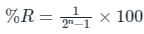
The percentage resolution (%R) of an n-bit DAC is:
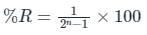
The percentage resolution (%R) of an n-bit DAC is:
Calculation:
As we know the formula resolution,
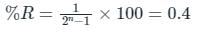
250 = 2N -1
2N = 251 ≈ 255
i.e., 28 = 255
N = 8
Hence the minimum value of N satisfying the condition.
As we know the formula resolution,
250 = 2N -1
2N = 251 ≈ 255
i.e., 28 = 255
N = 8
Hence the minimum value of N satisfying the condition.
A 8-bit A/D converter is used over a span of zero to 2.56 V. The binary representation of 1.0 V signal is- a)011 001 00
- b)011 100 01
- c)101 001 01
- d)101 000 10
Correct answer is option 'A'. Can you explain this answer?
A 8-bit A/D converter is used over a span of zero to 2.56 V. The binary representation of 1.0 V signal is
a)
011 001 00
b)
011 100 01
c)
101 001 01
d)
101 000 10
|
|
EduRev GATE answered |
Resolution:
Resolution of ADC is a change in analog voltage corresponding to a 1-bit increment.
Resolution is the number of bits per conversion cycle that the converter is capable of processing.

n = No. of bits of ADC
Vrange = Vmax - Vmin
Analog output = Reslotion x Decimal equivalent to binary
Vo = R x D
Resolution of ADC is a change in analog voltage corresponding to a 1-bit increment.
Resolution is the number of bits per conversion cycle that the converter is capable of processing.
n = No. of bits of ADC
Vrange = Vmax - Vmin
Analog output = Reslotion x Decimal equivalent to binary
Vo = R x D
Calculation:
Vrange = Vmax - Vmin
Vmax = 2.56 V
Vmin = 0 V
⇒ Vrange = 2.56 V
n = 8
Resolution is
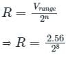
∴ R = 0.01.
Output voltage Vo = 1 V
⇒ 1 = 0.01 x D
∴ D = 100
The binary value of 100 is
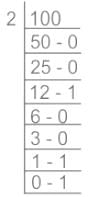
The binary equivalent of 100 is (011 001 00)2
Vrange = Vmax - Vmin
Vmax = 2.56 V
Vmin = 0 V
⇒ Vrange = 2.56 V
n = 8
Resolution is
∴ R = 0.01.
Output voltage Vo = 1 V
⇒ 1 = 0.01 x D
∴ D = 100
The binary value of 100 is
The binary equivalent of 100 is (011 001 00)2
The time required to complete the conversion of Analog to Digital is ________ the duration of the hold mode of S/H.- a)Greater than
- b)Equals to
- c)Less than
- d)Greater than or Equals to
Correct answer is option 'C'. Can you explain this answer?
The time required to complete the conversion of Analog to Digital is ________ the duration of the hold mode of S/H.
a)
Greater than
b)
Equals to
c)
Less than
d)
Greater than or Equals to
|
|
EduRev GATE answered |
The A/D converter begins the conversion after it receives a convert command. The time required to complete the conversion should be less than the duration of the hold mode of S/H.
In A/D converter, what is the time relation between sampling period T and the duration of the sample mode and the hold mode?- a)Should be larger than the duration of sample mode and hold mode
- b)Should be smaller than the duration of sample mode and hold mode
- c)Should be equal to the duration of sample mode and hold mode
- d)Should be larger than or equals to the duration of sample mode and hold mode
Correct answer is option 'A'. Can you explain this answer?
In A/D converter, what is the time relation between sampling period T and the duration of the sample mode and the hold mode?
a)
Should be larger than the duration of sample mode and hold mode
b)
Should be smaller than the duration of sample mode and hold mode
c)
Should be equal to the duration of sample mode and hold mode
d)
Should be larger than or equals to the duration of sample mode and hold mode
|
|
EduRev GATE answered |
The A/D converter begins the conversion after it receives a convert command. The sampling period T should be larger than the duration of the sample mode and the hold mode.
For a given sample-and-hold circuit, if the value of the hold capacitor is increased, then- a)droop rate decreases and acquisition time decreases
- b)droop rate decreases and acquisition time increases
- c)droop rate increases and acquisition time decreases
- d)droop rate increases and acquisition time increases
Correct answer is option 'B'. Can you explain this answer?
For a given sample-and-hold circuit, if the value of the hold capacitor is increased, then
a)
droop rate decreases and acquisition time decreases
b)
droop rate decreases and acquisition time increases
c)
droop rate increases and acquisition time decreases
d)
droop rate increases and acquisition time increases
|
|
EduRev GATE answered |
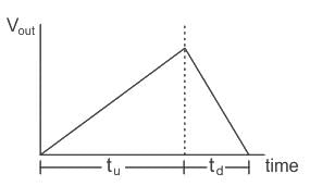
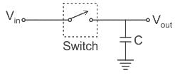
Concepts:
Generally, a sample & hold circuit is designed using an opamp. The given circuit shows the general implementation:
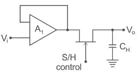
Sample & Hold circuit capacitor CH is charged by the Amplifier A1.
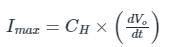
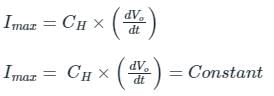
The maximum output current of the opamp is given as:
Sample & Hold circuit capacitor CH is charged by the Amplifier A1.
The maximum output current of the opamp is given as:
Droop rate
 when V0 is the voltage at the steady state.
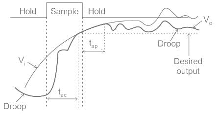
The acquisition time (tac) is depicted in the following figure:
Analylsis:
If CH increases then ‘t’ which is the acquiring time must also increase to maintain the relationship.
Also, capacitor discharging time constant TC(discharge) is proportional to capacitance i.e.
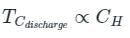
So if CH increases then capacitor voltage decreases slowly because of discharging time constant, this means droop rate decreases.
Also, capacitor discharging time constant TC(discharge) is proportional to capacitance i.e.
So if CH increases then capacitor voltage decreases slowly because of discharging time constant, this means droop rate decreases.
Figure shows 4 block diagram of a system to recover a sampled signal shown as input.
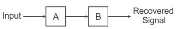
Blocks A and B can be respectively :- a)Zero order hold and low pass filter
- b)Multiplier and high pass filter
- c)Envelop detector and sampler
- d)Tuned circuit and mixer
Correct answer is option 'A'. Can you explain this answer?
Figure shows 4 block diagram of a system to recover a sampled signal shown as input.
Blocks A and B can be respectively :
Blocks A and B can be respectively :
a)
Zero order hold and low pass filter
b)
Multiplier and high pass filter
c)
Envelop detector and sampler
d)
Tuned circuit and mixer
|
|
EduRev GATE answered |
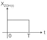
Zero-order hold circuit:
It is a mathematical model of two practical signal Reconstruction done by convention Digital to Analog converter (DAC).
By holding each sample value for one sample interval it converts the discrete signal into an analog signal.
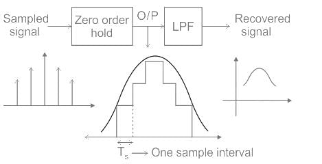
By holding each sample value for one sample interval it converts the discrete signal into an analog signal.
Important Points
Zero-order function 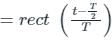
A good Sample and Hold circuit should have - High input impedance
- High output impedance
- Low input impedance
- Low output impedance
- a)1 and 2 only
- b)2 and 3 only
- c)3 and 4 only
- d)1 and 4 only
Correct answer is option 'D'. Can you explain this answer?
A good Sample and Hold circuit should have
- High input impedance
- High output impedance
- Low input impedance
- Low output impedance
a)
1 and 2 only
b)
2 and 3 only
c)
3 and 4 only
d)
1 and 4 only
|
|
EduRev GATE answered |
Sample and Hold (S/H) circuit:
It is used with an analog to digital converter to sample the input analog signal and hold the sample signal.
Circuit:-
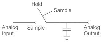
Properties:
1. A S/H Circuit should have high input impedance and low output impedance because due to high input impedance loading effect [It is the degree to which a measurement instrument impact electrical properties (Voltage, Current, resistance) of a Circuit] is less and Circuit performance is better.
1. A S/H Circuit should have high input impedance and low output impedance because due to high input impedance loading effect [It is the degree to which a measurement instrument impact electrical properties (Voltage, Current, resistance) of a Circuit] is less and Circuit performance is better.
Conclusions:
for better circuit performance input impedance should be high and output impedance should be low.
for better circuit performance input impedance should be high and output impedance should be low.
Option 4 correct choice.
Sample-and-hold circuits in ADCs are designed to:- a)sample and hold the output of the binary counter during the conversion process
- b)stabilize the ADCs threshold voltage during the conversion process
- c)stabilize the input analog signal during the conversion process
- d)sample and hold the ADC staircase waveform during the conversion process
Correct answer is option 'C'. Can you explain this answer?
Sample-and-hold circuits in ADCs are designed to:
a)
sample and hold the output of the binary counter during the conversion process
b)
stabilize the ADCs threshold voltage during the conversion process
c)
stabilize the input analog signal during the conversion process
d)
sample and hold the ADC staircase waveform during the conversion process
|
|
EduRev GATE answered |
Sample & Hold Circuit is used to sample the given input signal and to hold the sampled value.
Sample and hold circuit is used to sample an analog signal for a short interval of time in the range of 1 to 10 µS and to hold on to its last sampled value, until the input signal is sampled again.
The holding period may be from a few milliseconds to several seconds.
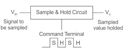
Sample and hold circuit is used to sample an analog signal for a short interval of time in the range of 1 to 10 µS and to hold on to its last sampled value, until the input signal is sampled again.
The holding period may be from a few milliseconds to several seconds.
Applications of Sample & Hold circuits:
- Out of different ADCs, successive approximation type ADC uses an S/H circuit, where the signal is to be held constant while A to D conversion is taking place.
- They are also used in DACs for the same purpose.
- It is used in analog demultiplexing in data distribution and in analog delay lines.
- In general, S/H circuits are used in all applications where it is necessary to stabilize the analog signal for further processing.
A D/A converter has 5V full-scale input voltage and an accuracy of ± 0.2%. The maximum error for any output voltage will be- a)5 mV
- b)10 mV
- c)20 mV
- d)1 mV
Correct answer is option 'B'. Can you explain this answer?
A D/A converter has 5V full-scale input voltage and an accuracy of ± 0.2%. The maximum error for any output voltage will be
a)
5 mV
b)
10 mV
c)
20 mV
d)
1 mV
|
|
EduRev GATE answered |
Concept:
Maximum error (Er) of D/A is given as,
Er = (VFS x Accuracy)
Where,
VFS: full-scale input voltage
Calculation:
Given: VfS = 5V , Accuracy= 0.2%

Er = 10 mV
Maximum error (Er) of D/A is given as,
Er = (VFS x Accuracy)
Where,
VFS: full-scale input voltage
Calculation:
Given: VfS = 5V , Accuracy= 0.2%
Er = 10 mV
What is the maximum conversion time for an n-bit counting ADC? - a)2n + 1 clock cycles
- b)2n - 1 clock cycles
- c)2n - 1 clock cycles
- d)2n + 1 clock cycles
Correct answer is option 'B'. Can you explain this answer?
What is the maximum conversion time for an n-bit counting ADC?
a)
2n + 1 clock cycles
b)
2n - 1 clock cycles
c)
2n - 1 clock cycles
d)
2n + 1 clock cycles
|
|
EduRev GATE answered |
Concept:
Digital ramp ADC conversion time is given as:
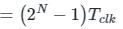
Important Points
The conversion time of different types of n-bit ADC is shown:
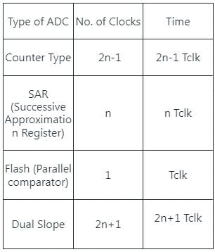
The conversion time of different types of n-bit ADC is shown:
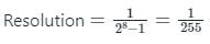
The resolution of an 8 bit DAC will be:- a)1/255
- b)1/8
- c)1/128
- d)1/64
Correct answer is option 'A'. Can you explain this answer?
The resolution of an 8 bit DAC will be:
a)
1/255
b)
1/8
c)
1/128
d)
1/64
|
|
EduRev GATE answered |
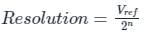
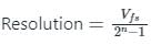
Resolution: It is defined as the smallest change in the analog output voltage corresponding to a change of one bit in the digital input.
The percentage resolution (%R) of an n-bit DAC is:
The resolution of an n-bit DAC with a range of output voltage from 0 to V is given by:
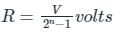
The resolution of an n-bit DAC with a range of output voltage from 0 to V is given by:
Calculation:
Number of bits (n) = 8
When a time-varying signal has to be digitized using an ADC, which of the following is necessary to use before digitization?- a)Time division multiplexer
- b)Frequency division multiplexer
- c)Sample and hold circuit
- d)Instrument amplifier
Correct answer is option 'C'. Can you explain this answer?
When a time-varying signal has to be digitized using an ADC, which of the following is necessary to use before digitization?
a)
Time division multiplexer
b)
Frequency division multiplexer
c)
Sample and hold circuit
d)
Instrument amplifier
|
|
EduRev GATE answered |
Sample and Hold circuit:
It samples the incoming analog signal and holds this sample values for a certain instant of time.
In the basic circuit diagram, an analog switch and a capacitor is used to perform the work.
It samples the incoming analog signal and holds this sample values for a certain instant of time.
In the basic circuit diagram, an analog switch and a capacitor is used to perform the work.
In this circuit, the switch can be either BJT, MOSFET, etc.
When the switch is closed by the applied input signal, the capacitor starts charging and holds the sampled value and the sampling interval is the same as the charging duration of the capacitor.
The capacitor holds the sampled value for half interval and changes its value in another half interval of time.
Application of sample and hold circuit
Analog to digital converter
- Signal processing
- Filter design
- Oscilloscope
Explanation:
When a time varying signal has to be digitized using an ADC, sample and hold circuit is necessary to use before digitation. Because sample and hold circuit take sample at particular instant.
When a time varying signal has to be digitized using an ADC, sample and hold circuit is necessary to use before digitation. Because sample and hold circuit take sample at particular instant.
A signal channel signal acquisition system with 0-10 V range consist of a sample and hold circuit with worst case drop rate of 100 μV/ms and 10 bit ADC. The maximum conversion time for the ADC is- a)49 ms
- b)0.49 ms
- c)4.9 ms
- d)490 ms
Correct answer is option 'A'. Can you explain this answer?
A signal channel signal acquisition system with 0-10 V range consist of a sample and hold circuit with worst case drop rate of 100 μV/ms and 10 bit ADC. The maximum conversion time for the ADC is
a)
49 ms
b)
0.49 ms
c)
4.9 ms
d)
490 ms
|
|
EduRev GATE answered |
In an ADC along with sample and hold circuit, for avoiding error at the output, the voltage of the capacitor should be not dropped by more than ± Δ/2
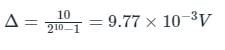
Δ/2 = 4.88 × 10³ V
Maximum conversation time for the ADC is
Δ/2 = 4.88 × 10³ V
Maximum conversation time for the ADC is
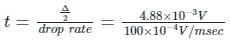
= 48.87 msec ≈ 49 msec
The smallest change in the input signal that can be detected by an instrument is called- a)Accuracy
- b)Sensitivity
- c)Resolution
- d)Precision
Correct answer is option 'C'. Can you explain this answer?
The smallest change in the input signal that can be detected by an instrument is called
a)
Accuracy
b)
Sensitivity
c)
Resolution
d)
Precision
|
|
EduRev GATE answered |
- The smallest change in the input signal that can be detected by an instrument is referred to as its "resolution."
- The term resolution describes the finest detail that a device or system can detect or measure.
- It is a key parameter for systems that deal with digital signals, as it is directly linked to the quality or level of detail of the output.
What is the main function of (A/D) or ADC converter?- a)Converts Digital to Analog Signal
- b)Converts Analog to Digital signal
- c)All of the mentioned
- d)None of the mentioned
Correct answer is option 'B'. Can you explain this answer?
What is the main function of (A/D) or ADC converter?
a)
Converts Digital to Analog Signal
b)
Converts Analog to Digital signal
c)
All of the mentioned
d)
None of the mentioned
|
|
EduRev GATE answered |
The electronic device that performs this conversion from an analog signal to a digital sequence is called an analog-to-digital (A/D) converter (ADC).
Identify the most significant bit from the '100010' binary data.- a)Right most bit 0
- b)Second bit from side 0
- c)Central bit 0
- d)Left most bit 1
Correct answer is option 'D'. Can you explain this answer?
Identify the most significant bit from the '100010' binary data.
a)
Right most bit 0
b)
Second bit from side 0
c)
Central bit 0
d)
Left most bit 1
|
|
EduRev GATE answered |
MSB stands for most significant bit is the bit position in a binary number having the greatest value.
The MSB is sometimes referred to as the high-order bit or left-most bit due to the convention in positional notation of writing more significant digits further to the left.
The MSB can also correspond to the sign bit of a signed binary number. In one's and two's complement notation, "1" signifies a negative number and "0" signifies a positive number.
Example:
(12)10 = (1100)2
(12)10 = (1100)2
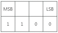
According to the question, the most significant bit of '100010' binary data is '1'.
For a 10-bit digital ramp ADC using 500 kHz clock, the maximum conversion time is- a)2048 μs
- b)2064 μs
- c)2046 μs
- d)2084 μs
Correct answer is option 'C'. Can you explain this answer?
For a 10-bit digital ramp ADC using 500 kHz clock, the maximum conversion time is
a)
2048 μs
b)
2064 μs
c)
2046 μs
d)
2084 μs
|
|
Telecom Tuners answered |
Concept:
Digital ramp ADC conversion time is given as:
Given:
n = 10
f = 500 kHz
Given:
n = 10
f = 500 kHz
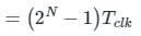
Analysis:
= 2 μs
Conversion time = (2N – 1) Tclk
(1024 - 1) × 2 μs = 2046 μs
= 2 μs
Conversion time = (2N – 1) Tclk
(1024 - 1) × 2 μs = 2046 μs
Important Points
The conversion time of different types of n-bit ADC is shown :
Chapter doubts & questions for A/D & D/A Converters and Sample/Hold Circuits - Analog and Digital Electronics 2025 is part of Electrical Engineering (EE) exam preparation. The chapters have been prepared according to the Electrical Engineering (EE) exam syllabus. The Chapter doubts & questions, notes, tests & MCQs are made for Electrical Engineering (EE) 2025 Exam. Find important definitions, questions, notes, meanings, examples, exercises, MCQs and online tests here.
Chapter doubts & questions of A/D & D/A Converters and Sample/Hold Circuits - Analog and Digital Electronics in English & Hindi are available as part of Electrical Engineering (EE) exam.
Download more important topics, notes, lectures and mock test series for Electrical Engineering (EE) Exam by signing up for free.
Analog and Digital Electronics
135 videos|167 docs|71 tests
|
|
© EduRev
|
Education Revolution
|


|


Signup to see your scores
go up within 7 days!
Access 1000+ FREE Docs, Videos and Tests
Takes less than 10 seconds to signup