


Electronics and Communication Engineering (ECE) Exam > Electronics and Communication Engineering (ECE) Questions > The built-in potential of a P N junction diod...
Start Learning for Free

The built-in potential of a P N junction diode is 0.7 V at room temperature. What will be the approximate value of built-in potential if the doping concentrations on both sides are doubled?
Assume In (2) = 0.7
Assume In (2) = 0.7
- a)0.9846 V
- b)0.73604 V
- c)0.7182V
- d)0.49 V
Correct answer is option 'B'. Can you explain this answer?
| FREE This question is part of | Download PDF Attempt this Test |
Most Upvoted Answer
The built-in potential of a P N junction diode is 0.7 V at room temper...
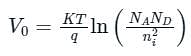
The built-in potential of a P-N junction diode is determined by the difference in the work functions of the P and N regions. It is given by the formula:
\(V_{bi} = \frac{kT}{q} \ln \left( \frac{N_AN_D}{n_i^2} \right)\)
where:
- \(V_{bi}\) is the built-in potential
- \(k\) is the Boltzmann constant
- \(T\) is the temperature in Kelvin
- \(q\) is the elementary charge
- \(N_A\) and \(N_D\) are the doping concentrations of the P and N regions, respectively
- \(n_i\) is the intrinsic carrier concentration
In this question, we are given that the built-in potential is 0.7 V at room temperature. Let's assume the room temperature is 300 K.
To find the approximate value of the built-in potential if the doping concentrations on both sides are doubled, we need to calculate the new value of \(V_{bi}\) using the formula above.
Doubling the doping concentrations means that \(N_A\) and \(N_D\) are both multiplied by 2.
Let's plug in the values into the formula:
\(V_{bi2} = \frac{kT}{q} \ln \left( \frac{2N_AN_D}{n_i^2} \right)\)
Since we are only interested in the approximate value, we can use the approximation \(\ln(2x) \approx \ln(x) + \ln(2)\).
\(V_{bi2} = \frac{kT}{q} \left( \ln \left( \frac{N_AN_D}{n_i^2} \right) + \ln(2) \right)\)
The term \(\ln \left( \frac{N_AN_D}{n_i^2} \right)\) is the same as the term in the original formula, which gives the built-in potential at room temperature. Let's call this term \(V_{bi1}\):
\(V_{bi1} = \frac{kT}{q} \ln \left( \frac{N_AN_D}{n_i^2} \right)\)
Therefore, we can rewrite the equation as:
\(V_{bi2} = V_{bi1} + \frac{kT}{q} \ln(2)\)
Substituting the values, we get:
\(V_{bi2} = 0.7 + \frac{(1.38 \times 10^{-23} \times 300)}{(1.6 \times 10^{-19})} \times \ln(2)\)
\(V_{bi2} \approx 0.73604\) V
Therefore, the approximate value of the built-in potential if the doping concentrations on both sides are doubled is 0.73604 V.
Free Test
FREE
| Start Free Test |
Community Answer
The built-in potential of a P N junction diode is 0.7 V at room temper...
Concept:
- As the N-type material has lost electrons and the P-type has lost holes, the N-type material has become positive with respect to the P-type.
- Then the presence of impurity ions on both sides of the junction causes an electric field to be established across this region with the N-side at a positive voltage relative to the P-side.
- The problem now is that a free charge requires some extra energy to overcome the barrier that now exists for it to be able to cross the depletion region junction.
- This electric field created by the diffusion process has created a “built-in potential difference” across the junction with an open-circuit (zero bias) potential
Calculation:
Given built-in voltage of the diode is 0.7 V
Now doping concentrations on both sides are doubled. i.e, NA’ = 2NA and ND’ = 2ND
Newly built-in potential is:
Given built-in voltage of the diode is 0.7 V
Now doping concentrations on both sides are doubled. i.e, NA’ = 2NA and ND’ = 2ND
Newly built-in potential is:

Attention Electronics and Communication Engineering (ECE) Students!
To make sure you are not studying endlessly, EduRev has designed Electronics and Communication Engineering (ECE) study material, with Structured Courses, Videos, & Test Series. Plus get personalized analysis, doubt solving and improvement plans to achieve a great score in Electronics and Communication Engineering (ECE).


|
Explore Courses for Electronics and Communication Engineering (ECE) exam
|
|
Similar Electronics and Communication Engineering (ECE) Doubts


Top Courses for Electronics and Communication Engineering (ECE)View all


The built-in potential of a P N junction diode is 0.7 V at room temperature. What will be the approximate value of built-in potential if the doping concentrations on both sides are doubled?Assume In (2) = 0.7a)0.9846 Vb)0.73604Vc)0.7182Vd)0.49VCorrect answer is option 'B'. Can you explain this answer?
Question Description
The built-in potential of a P N junction diode is 0.7 V at room temperature. What will be the approximate value of built-in potential if the doping concentrations on both sides are doubled?Assume In (2) = 0.7a)0.9846 Vb)0.73604Vc)0.7182Vd)0.49VCorrect answer is option 'B'. Can you explain this answer? for Electronics and Communication Engineering (ECE) 2024 is part of Electronics and Communication Engineering (ECE) preparation. The Question and answers have been prepared according to the Electronics and Communication Engineering (ECE) exam syllabus. Information about The built-in potential of a P N junction diode is 0.7 V at room temperature. What will be the approximate value of built-in potential if the doping concentrations on both sides are doubled?Assume In (2) = 0.7a)0.9846 Vb)0.73604Vc)0.7182Vd)0.49VCorrect answer is option 'B'. Can you explain this answer? covers all topics & solutions for Electronics and Communication Engineering (ECE) 2024 Exam. Find important definitions, questions, meanings, examples, exercises and tests below for The built-in potential of a P N junction diode is 0.7 V at room temperature. What will be the approximate value of built-in potential if the doping concentrations on both sides are doubled?Assume In (2) = 0.7a)0.9846 Vb)0.73604Vc)0.7182Vd)0.49VCorrect answer is option 'B'. Can you explain this answer?.
The built-in potential of a P N junction diode is 0.7 V at room temperature. What will be the approximate value of built-in potential if the doping concentrations on both sides are doubled?Assume In (2) = 0.7a)0.9846 Vb)0.73604Vc)0.7182Vd)0.49VCorrect answer is option 'B'. Can you explain this answer? for Electronics and Communication Engineering (ECE) 2024 is part of Electronics and Communication Engineering (ECE) preparation. The Question and answers have been prepared according to the Electronics and Communication Engineering (ECE) exam syllabus. Information about The built-in potential of a P N junction diode is 0.7 V at room temperature. What will be the approximate value of built-in potential if the doping concentrations on both sides are doubled?Assume In (2) = 0.7a)0.9846 Vb)0.73604Vc)0.7182Vd)0.49VCorrect answer is option 'B'. Can you explain this answer? covers all topics & solutions for Electronics and Communication Engineering (ECE) 2024 Exam. Find important definitions, questions, meanings, examples, exercises and tests below for The built-in potential of a P N junction diode is 0.7 V at room temperature. What will be the approximate value of built-in potential if the doping concentrations on both sides are doubled?Assume In (2) = 0.7a)0.9846 Vb)0.73604Vc)0.7182Vd)0.49VCorrect answer is option 'B'. Can you explain this answer?.
Solutions for The built-in potential of a P N junction diode is 0.7 V at room temperature. What will be the approximate value of built-in potential if the doping concentrations on both sides are doubled?Assume In (2) = 0.7a)0.9846 Vb)0.73604Vc)0.7182Vd)0.49VCorrect answer is option 'B'. Can you explain this answer? in English & in Hindi are available as part of our courses for Electronics and Communication Engineering (ECE).
Download more important topics, notes, lectures and mock test series for Electronics and Communication Engineering (ECE) Exam by signing up for free.
Here you can find the meaning of The built-in potential of a P N junction diode is 0.7 V at room temperature. What will be the approximate value of built-in potential if the doping concentrations on both sides are doubled?Assume In (2) = 0.7a)0.9846 Vb)0.73604Vc)0.7182Vd)0.49VCorrect answer is option 'B'. Can you explain this answer? defined & explained in the simplest way possible. Besides giving the explanation of
The built-in potential of a P N junction diode is 0.7 V at room temperature. What will be the approximate value of built-in potential if the doping concentrations on both sides are doubled?Assume In (2) = 0.7a)0.9846 Vb)0.73604Vc)0.7182Vd)0.49VCorrect answer is option 'B'. Can you explain this answer?, a detailed solution for The built-in potential of a P N junction diode is 0.7 V at room temperature. What will be the approximate value of built-in potential if the doping concentrations on both sides are doubled?Assume In (2) = 0.7a)0.9846 Vb)0.73604Vc)0.7182Vd)0.49VCorrect answer is option 'B'. Can you explain this answer? has been provided alongside types of The built-in potential of a P N junction diode is 0.7 V at room temperature. What will be the approximate value of built-in potential if the doping concentrations on both sides are doubled?Assume In (2) = 0.7a)0.9846 Vb)0.73604Vc)0.7182Vd)0.49VCorrect answer is option 'B'. Can you explain this answer? theory, EduRev gives you an
ample number of questions to practice The built-in potential of a P N junction diode is 0.7 V at room temperature. What will be the approximate value of built-in potential if the doping concentrations on both sides are doubled?Assume In (2) = 0.7a)0.9846 Vb)0.73604Vc)0.7182Vd)0.49VCorrect answer is option 'B'. Can you explain this answer? tests, examples and also practice Electronics and Communication Engineering (ECE) tests.
|
|
Explore Courses for Electronics and Communication Engineering (ECE) exam
|
|
Suggested Free Tests
Signup for Free!
Signup to see your scores go up within 7 days! Learn & Practice with 1000+ FREE Notes, Videos & Tests.


x
![]()
For Your Perfect Score in Electronics and Communication Engineering (ECE)
The Best you need at One Place
|
© EduRev
|
Education Revolution
|


Follow Us
|


Signup to see your scores
go up within 7 days!
Access 1000+ FREE Docs, Videos and Tests
Takes less than 10 seconds to signup