Electronics and Communication Engineering (ECE) Exam > Electronics and Communication Engineering (ECE) Questions > A silicon P-N junction is shown in the figure...
Start Learning for Free
A silicon P-N junction is shown in the figure. The doping in the P region is 5×1016cm−3 and doping in the N region is 10 ×1016 cm−3 . The parameters given are
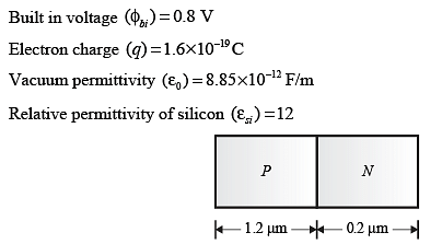
The magnitude of reverse bias voltage that would completely deplete one of the two regions (P or N) prior to the other (rounded off to one decimal place) is________ V.
Correct answer is '107.67'. Can you explain this answer?
| FREE This question is part of | Download PDF Attempt this Test |
Most Upvoted Answer
A silicon P-N junction is shown in the figure. The doping in the P reg...
Given
Doping in P-region NA =5*1016 cm-3
Doping in N-region ND =1017 cm-3
Given p-n junction is shown below,

So width of depletion region, W = Xn + Xp
From charge equality concept,
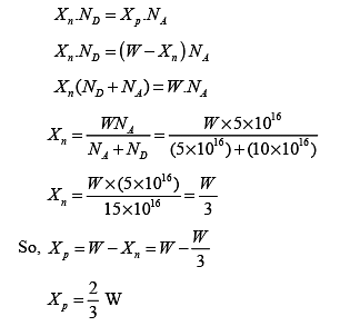
Suppose when N-is depleted completely, during reverse bias so,
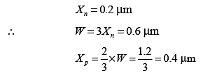
i.e. when N is depleted completely (i.e. 0.2 μm ) then and only then P side is depleted only by 0.4 μm only. Thus

So, total depletion width (W) under reverse bias is,
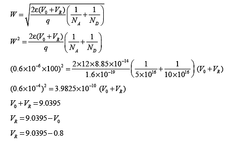
VR = 8.2395 V≈ 8.24 V
Thus, the magnitude of reverse bias voltage that would completely deplete N region is 8.24 V. Hence, the correct answer for VR is 8.24 V .
Question_Type: 4
Free Test
FREE
| Start Free Test |
Community Answer
A silicon P-N junction is shown in the figure. The doping in the P reg...
Given
Doping in P-region NA =5*1016 cm-3
Doping in N-region ND =1017 cm-3
Given p-n junction is shown below,

So width of depletion region, W = Xn + Xp
From charge equality concept,

Suppose when N-is depleted completely, during reverse bias so,

i.e. when N is depleted completely (i.e. 0.2 μm ) then and only then P side is depleted only by 0.4 μm only. Thus

So, total depletion width (W) under reverse bias is,

VR = 8.2395 V≈ 8.24 V
Thus, the magnitude of reverse bias voltage that would completely deplete N region is 8.24 V. Hence, the correct answer for VR is 8.24 V .
Question_Type: 4
Attention Electronics and Communication Engineering (ECE) Students!
To make sure you are not studying endlessly, EduRev has designed Electronics and Communication Engineering (ECE) study material, with Structured Courses, Videos, & Test Series. Plus get personalized analysis, doubt solving and improvement plans to achieve a great score in Electronics and Communication Engineering (ECE).

|
Explore Courses for Electronics and Communication Engineering (ECE) exam
|

|
Similar Electronics and Communication Engineering (ECE) Doubts
A silicon P-N junction is shown in the figure. The doping in the P region is 5×1016cm−3 and doping in the N region is 10 ×1016 cm−3 . The parameters given areThe magnitude of reverse bias voltage that would completely deplete one of the two regions (P or N) prior to the other (rounded off to one decimal place) is________ V.Correct answer is '107.67'. Can you explain this answer?
Question Description
A silicon P-N junction is shown in the figure. The doping in the P region is 5×1016cm−3 and doping in the N region is 10 ×1016 cm−3 . The parameters given areThe magnitude of reverse bias voltage that would completely deplete one of the two regions (P or N) prior to the other (rounded off to one decimal place) is________ V.Correct answer is '107.67'. Can you explain this answer? for Electronics and Communication Engineering (ECE) 2024 is part of Electronics and Communication Engineering (ECE) preparation. The Question and answers have been prepared according to the Electronics and Communication Engineering (ECE) exam syllabus. Information about A silicon P-N junction is shown in the figure. The doping in the P region is 5×1016cm−3 and doping in the N region is 10 ×1016 cm−3 . The parameters given areThe magnitude of reverse bias voltage that would completely deplete one of the two regions (P or N) prior to the other (rounded off to one decimal place) is________ V.Correct answer is '107.67'. Can you explain this answer? covers all topics & solutions for Electronics and Communication Engineering (ECE) 2024 Exam. Find important definitions, questions, meanings, examples, exercises and tests below for A silicon P-N junction is shown in the figure. The doping in the P region is 5×1016cm−3 and doping in the N region is 10 ×1016 cm−3 . The parameters given areThe magnitude of reverse bias voltage that would completely deplete one of the two regions (P or N) prior to the other (rounded off to one decimal place) is________ V.Correct answer is '107.67'. Can you explain this answer?.
A silicon P-N junction is shown in the figure. The doping in the P region is 5×1016cm−3 and doping in the N region is 10 ×1016 cm−3 . The parameters given areThe magnitude of reverse bias voltage that would completely deplete one of the two regions (P or N) prior to the other (rounded off to one decimal place) is________ V.Correct answer is '107.67'. Can you explain this answer? for Electronics and Communication Engineering (ECE) 2024 is part of Electronics and Communication Engineering (ECE) preparation. The Question and answers have been prepared according to the Electronics and Communication Engineering (ECE) exam syllabus. Information about A silicon P-N junction is shown in the figure. The doping in the P region is 5×1016cm−3 and doping in the N region is 10 ×1016 cm−3 . The parameters given areThe magnitude of reverse bias voltage that would completely deplete one of the two regions (P or N) prior to the other (rounded off to one decimal place) is________ V.Correct answer is '107.67'. Can you explain this answer? covers all topics & solutions for Electronics and Communication Engineering (ECE) 2024 Exam. Find important definitions, questions, meanings, examples, exercises and tests below for A silicon P-N junction is shown in the figure. The doping in the P region is 5×1016cm−3 and doping in the N region is 10 ×1016 cm−3 . The parameters given areThe magnitude of reverse bias voltage that would completely deplete one of the two regions (P or N) prior to the other (rounded off to one decimal place) is________ V.Correct answer is '107.67'. Can you explain this answer?.
Solutions for A silicon P-N junction is shown in the figure. The doping in the P region is 5×1016cm−3 and doping in the N region is 10 ×1016 cm−3 . The parameters given areThe magnitude of reverse bias voltage that would completely deplete one of the two regions (P or N) prior to the other (rounded off to one decimal place) is________ V.Correct answer is '107.67'. Can you explain this answer? in English & in Hindi are available as part of our courses for Electronics and Communication Engineering (ECE).
Download more important topics, notes, lectures and mock test series for Electronics and Communication Engineering (ECE) Exam by signing up for free.
Here you can find the meaning of A silicon P-N junction is shown in the figure. The doping in the P region is 5×1016cm−3 and doping in the N region is 10 ×1016 cm−3 . The parameters given areThe magnitude of reverse bias voltage that would completely deplete one of the two regions (P or N) prior to the other (rounded off to one decimal place) is________ V.Correct answer is '107.67'. Can you explain this answer? defined & explained in the simplest way possible. Besides giving the explanation of
A silicon P-N junction is shown in the figure. The doping in the P region is 5×1016cm−3 and doping in the N region is 10 ×1016 cm−3 . The parameters given areThe magnitude of reverse bias voltage that would completely deplete one of the two regions (P or N) prior to the other (rounded off to one decimal place) is________ V.Correct answer is '107.67'. Can you explain this answer?, a detailed solution for A silicon P-N junction is shown in the figure. The doping in the P region is 5×1016cm−3 and doping in the N region is 10 ×1016 cm−3 . The parameters given areThe magnitude of reverse bias voltage that would completely deplete one of the two regions (P or N) prior to the other (rounded off to one decimal place) is________ V.Correct answer is '107.67'. Can you explain this answer? has been provided alongside types of A silicon P-N junction is shown in the figure. The doping in the P region is 5×1016cm−3 and doping in the N region is 10 ×1016 cm−3 . The parameters given areThe magnitude of reverse bias voltage that would completely deplete one of the two regions (P or N) prior to the other (rounded off to one decimal place) is________ V.Correct answer is '107.67'. Can you explain this answer? theory, EduRev gives you an
ample number of questions to practice A silicon P-N junction is shown in the figure. The doping in the P region is 5×1016cm−3 and doping in the N region is 10 ×1016 cm−3 . The parameters given areThe magnitude of reverse bias voltage that would completely deplete one of the two regions (P or N) prior to the other (rounded off to one decimal place) is________ V.Correct answer is '107.67'. Can you explain this answer? tests, examples and also practice Electronics and Communication Engineering (ECE) tests.

|
Explore Courses for Electronics and Communication Engineering (ECE) exam
|

|
Suggested Free Tests
Signup for Free!
Signup to see your scores go up within 7 days! Learn & Practice with 1000+ FREE Notes, Videos & Tests.


