


All Exams >
UPSC >
Electrical Engineering Optional Notes for UPSC >
All Questions
All questions of Amplifiers for UPSC CSE Exam
A FET circuit has a transconductance of 2500 µ seconds and drain resistance equals to 10Kohms than voltage gain will be __________- a)20
- b)25
- c)30
- d)35
Correct answer is option 'B'. Can you explain this answer?
A FET circuit has a transconductance of 2500 µ seconds and drain resistance equals to 10Kohms than voltage gain will be __________
a)
20
b)
25
c)
30
d)
35

|
Pioneer Academy answered |
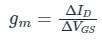
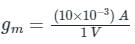
The transconductance, gm is defined as
gm = ΔID / ΔVGS
so gm = Voltage gain / RD
Therefore, voltage gain = gm x RD
= 2500 x 10-6 x 10 x 103
= 25.
gm = ΔID / ΔVGS
so gm = Voltage gain / RD
Therefore, voltage gain = gm x RD
= 2500 x 10-6 x 10 x 103
= 25.

In a Common Drain (CD) MOSFET amplifier with voltage divider bias with R1 and R2 equal to 1.5 MΩ and 1 MΩ respectively, the input impedance Zf is:- a)220 kΩ
- b)600 kΩ
- c)470 kΩ
- d)200 kΩ
Correct answer is option 'B'. Can you explain this answer?
In a Common Drain (CD) MOSFET amplifier with voltage divider bias with R1 and R2 equal to 1.5 MΩ and 1 MΩ respectively, the input impedance Zf is:
a)
220 kΩ
b)
600 kΩ
c)
470 kΩ
d)
200 kΩ
|
|
Sanjana Chopra answered |
Calculation of Input Impedance Zf:
- The input impedance Zf of a CD MOSFET amplifier with voltage divider bias can be calculated using the formula:
Zf = R1 || R2 + (1 + g_m * (R1 || R2))^-1
- Given that R1 = 1.5 MΩ and R2 = 1 MΩ, we can substitute these values into the formula.
Calculating R1 || R2:
- R1 || R2 = (R1 * R2) / (R1 + R2)
- R1 || R2 = (1.5 MΩ * 1 MΩ) / (1.5 MΩ + 1 MΩ)
- R1 || R2 = 1.5 MΩ * 1 MΩ / 2.5 MΩ
- R1 || R2 = 0.6 MΩ = 600 kΩ
Calculating g_m:
- Given parameters of the MOSFET and biasing conditions, the transconductance g_m is typically provided in the problem statement.
Substitute into the Input Impedance Formula:
- Zf = 600 kΩ + (1 + g_m * 600 kΩ)^-1
Final Calculation:
- Since we are given the options, we can calculate the input impedance for each option and find that the correct answer is option 'B' 600 kΩ.
Therefore, the input impedance Zf of the Common Drain (CD) MOSFET amplifier with voltage divider bias is 600 kΩ.
Consider a voltage series feedback network, where amplifier gain = 100, feedback factor = 5. For the basic amplifier, input voltage = 4V, input current=2mA. Find the input resistance of the network.- a)1.002kΩ
- b)1002kΩ
- c)2kΩ
- d)2000kΩ
Correct answer is option 'B'. Can you explain this answer?
Consider a voltage series feedback network, where amplifier gain = 100, feedback factor = 5. For the basic amplifier, input voltage = 4V, input current=2mA. Find the input resistance of the network.
a)
1.002kΩ
b)
1002kΩ
c)
2kΩ
d)
2000kΩ

|
Athul Das answered |
To find the input resistance of the network, we can use the formula:
Input resistance (Rin) = (Voltage gain / Current gain) * (Feedback factor / Amplifier gain)
Given:
Amplifier gain (Av) = 100
Feedback factor (β) = 5
The voltage gain (Av) can be calculated as the ratio of output voltage (Vo) to input voltage (Vi):
Av = Vo / Vi
Since it is a voltage series feedback network, the output voltage (Vo) and input voltage (Vi) are related by the formula:
Vo = Vi / (1 + β * Av)
Substituting the given values:
Av = 100
β = 5
Vo = Vi / (1 + 5 * 100)
Vo = Vi / 501
Now, we can calculate the output voltage (Vo) using the formula:
Vo = Av * Vi
Vo = 100 * 4V
Vo = 400V
Substituting the calculated values into the equation for Vo:
400V = Vi / 501
Solving for Vi:
Vi = 400V * 501
Vi = 200,400V
Now, we can substitute the calculated values into the formula for input resistance (Rin):
Rin = (Av / Ai) * (β / Av)
Rin = (100 / (2mA / 200,400V)) * (5 / 100)
Rin = (100 / (0.002A / 200,400V)) * (5 / 100)
Rin = (100 / (0.002A / 200,400V)) * (5 / 100)
Rin = (100 / (0.002A / 200,400V)) * (5 / 100)
Rin = (100 / 0.002A) * (5 / 100)
Rin = (100 / 0.002A) * (5 / 100)
Rin = (100 / 0.002A) * (5 / 100)
Rin = (100 / 0.002A) * (5 / 100)
Rin = (100 / 0.002A) * (5 / 100)
Rin = 1,000 * 0.05
Rin = 50
Therefore, the input resistance of the network is 50 ohms.
If Av, Ai and Ap represents the voltage gain, current gain and power gain ratio of an amplifier which of the below is not the correct expression for the corresponding values in decibel?- a)Current gain: 20 log Ai db
- b)Voltage gain: 20 log Av db
- c)Power gain: 20 log Ap db
- d) Power gain: 10 log Ap
Correct answer is option 'C'. Can you explain this answer?
If Av, Ai and Ap represents the voltage gain, current gain and power gain ratio of an amplifier which of the below is not the correct expression for the corresponding values in decibel?
a)
Current gain: 20 log Ai db
b)
Voltage gain: 20 log Av db
c)
Power gain: 20 log Ap db
d)
Power gain: 10 log Ap
|
|
Ravi Singh answered |
Power gain is given by 10 log Ap db.
The units of voltage gain is- a)It has no units, it is a ratio
- b)Decibels (db)
- c)All of the mentioned
- d)None of the mentioned
Correct answer is option 'A'. Can you explain this answer?
The units of voltage gain is
a)
It has no units, it is a ratio
b)
Decibels (db)
c)
All of the mentioned
d)
None of the mentioned

|
Saptarshi Nair answered |
Voltage gain (Vo) = output voltage/input voltage (Vi). It is also expresses as 20 log (Vo/Vi) db.
Compared to bipolar transistors, field effect transistors are NOT normally characterized by:- a)high input impedance
- b)a reverse-biased PN junction
- c)low input impedance
- d)low power consumption
Correct answer is option 'C'. Can you explain this answer?
Compared to bipolar transistors, field effect transistors are NOT normally characterized by:
a)
high input impedance
b)
a reverse-biased PN junction
c)
low input impedance
d)
low power consumption
|
|
Pioneer Academy answered |
The difference between FET and BJT is explained in the following table:
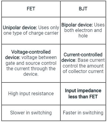
Hence, Option C is correct.
The ratio of the short circuit current gain of a current amplifier (Ai) to the open circuit voltage gain of a voltage amplifier (AV), given that both amplifiers have the same value of the input resistance (Ri) and output resistance (R0), is- a)Ri
- b) Ro
- c)Ri / R0
- d)Ro / Ri
Correct answer is option 'C'. Can you explain this answer?
The ratio of the short circuit current gain of a current amplifier (Ai) to the open circuit voltage gain of a voltage amplifier (AV), given that both amplifiers have the same value of the input resistance (Ri) and output resistance (R0), is
a)
Ri
b)
Ro
c)
Ri / R0
d)
Ro / Ri
|
|
Ravi Singh answered |
It is a standard mathematical relation.
The voltage gain of the amplifier is 8 and the current gain is 7. The power gain of the amplifier is- a)56 db
- b)17.481 db
- c)34.963 db
- d)1 db
Correct answer is option 'B'. Can you explain this answer?
The voltage gain of the amplifier is 8 and the current gain is 7. The power gain of the amplifier is
a)
56 db
b)
17.481 db
c)
34.963 db
d)
1 db

|
Jhanvi Choudhary answered |
The power gain is given by 10 log (7 X 8) db.
In a feedback network, input voltage is 14V, feedback voltage is 6V and source voltage is 20V. β is in ohms. What is its configuration?- a)Shunt-Shunt feedback
- b)Shunt-Series feedback
- c)Series-Series feedback
- d)Series-Shunt feedback
Correct answer is option 'C'. Can you explain this answer?
In a feedback network, input voltage is 14V, feedback voltage is 6V and source voltage is 20V. β is in ohms. What is its configuration?
a)
Shunt-Shunt feedback
b)
Shunt-Series feedback
c)
Series-Series feedback
d)
Series-Shunt feedback
|
|
Pioneer Academy answered |
Given that input is 14V, feedback is 6V and source is 20 V, we can see
VI = VS – VF, which is voltage mixing. Also, β is in ohms that is voltage/current.
Since output of feedback is voltage and input is current, the output has current sampling.
Thus, configuration is a series-series feedback/current – series feedback.
VI = VS – VF, which is voltage mixing. Also, β is in ohms that is voltage/current.
Since output of feedback is voltage and input is current, the output has current sampling.
Thus, configuration is a series-series feedback/current – series feedback.
What is the reverse transmission factor?- a)Ratio of output by input signal
- b)Ratio of feedback by input signal
- c)Ration of feedback by output signal
- d)Ratio of input by feedback signal
Correct answer is option 'C'. Can you explain this answer?
What is the reverse transmission factor?
a)
Ratio of output by input signal
b)
Ratio of feedback by input signal
c)
Ration of feedback by output signal
d)
Ratio of input by feedback signal
|
|
Athul Das answered |
The reverse transmission factor refers to the ratio of feedback by the output signal in a control system. It plays a crucial role in determining the stability and performance of the system. To understand this concept, let's break down the components of a control system and how they interact with each other.
1. Control system components:
a) Input signal: The desired or reference signal that the system aims to achieve.
b) Output signal: The measured or actual signal produced by the system.
c) Feedback signal: The portion of the output signal that is fed back to the system for comparison with the input signal.
d) Forward path: The path through which the input signal is processed to produce the output signal.
e) Feedback path: The path through which the feedback signal is combined with the input signal to generate an error signal.
2. Importance of feedback:
Feedback is essential in control systems as it allows for error correction and improves system performance. By comparing the output signal with the input signal, any discrepancies or errors can be detected, and appropriate adjustments can be made to minimize these errors.
3. Reverse transmission factor:
The reverse transmission factor, denoted as β, represents the ratio of feedback by the output signal. Mathematically, it can be expressed as:
β = Feedback signal / Output signal
4. Significance of the reverse transmission factor:
The reverse transmission factor influences the gain and stability of a control system. Here's why:
a) Gain: The gain of a system determines how much the output signal changes in response to a change in the input signal. The presence of feedback modifies the overall gain of the system. The reverse transmission factor affects the gain by determining the fraction of the output signal that is fed back into the system. A higher reverse transmission factor implies more feedback, leading to a reduction in the overall gain of the system.
b) Stability: Stability is a critical aspect of control systems. It refers to the ability of the system to maintain a steady output in the presence of disturbances or changes in the input signal. The reverse transmission factor plays a significant role in determining system stability. If the reverse transmission factor is too high, it can introduce instability into the system, causing oscillations or even system failure. Hence, it is crucial to carefully design the reverse transmission factor to ensure stability.
In summary, the reverse transmission factor represents the ratio of feedback by the output signal in a control system. It affects the gain and stability of the system and needs to be carefully considered during system design and analysis.
The output voltage of a voltage amplifier has been found to decrease by 20% when a load resistance of 1 kΩ is connected. What is the value of the amplifier output resistance?- a)50Ω
- b)200Ω
- c)250Ω
- d)350Ω
Correct answer is option 'C'. Can you explain this answer?
The output voltage of a voltage amplifier has been found to decrease by 20% when a load resistance of 1 kΩ is connected. What is the value of the amplifier output resistance?
a)
50Ω
b)
200Ω
c)
250Ω
d)
350Ω
|
|
Anshika Nambiar answered |
Ω is connected to its output. This means that the output voltage decreases by 20% when the load resistance is added.
When a 1 V increase in the gate voltage changes the drain current 10 mA in a FET, its gm equals.- a)0.01 mho
- b)100 mho
- c)1000 mho
- d)10000 mho
Correct answer is option 'A'. Can you explain this answer?
When a 1 V increase in the gate voltage changes the drain current 10 mA in a FET, its gm equals.
a)
0.01 mho
b)
100 mho
c)
1000 mho
d)
10000 mho
|
|
Pooja Patel answered |
Concept:
Transconductance indicates the amount of control the gate has on the drain current.
Mathematically, the transconductance (gm) is defined as:

It is given the name transconductance because it gives the relationship between the input voltage and the output current.
Calculation:
Given: Δ VGS = 1 V and Δ ID = 10 mA
∴ 
= 0.01 mho
Voltage gain of common drain amplifier is always slightly less than _____- a)0.5
- b)1
- c)1.5
- d)2
Correct answer is option 'B'. Can you explain this answer?
Voltage gain of common drain amplifier is always slightly less than _____
a)
0.5
b)
1
c)
1.5
d)
2
|
|
Pooja Patel answered |
In common drain amplifier
Writing KCL at the source node ;
Gm(vin – vout) – gmbs vout – gds vout = 0
vout vin = Gm / Gm + Gmbs + gds
Therefore gain is less than one.
Writing KCL at the source node ;
Gm(vin – vout) – gmbs vout – gds vout = 0
vout vin = Gm / Gm + Gmbs + gds
Therefore gain is less than one.
The gain of a FET amplifier can be changed by changing:- a)fm
- b)gm
- c)RL
- d)None of these
Correct answer is option 'B'. Can you explain this answer?
The gain of a FET amplifier can be changed by changing:
a)
fm
b)
gm
c)
RL
d)
None of these

|
Gate Funda answered |
Concept:
Voltage gain for a FET amplifier is given as:
AV = −gm(rd||RD)
Analysis:
Hence, The gain of a FET amplifier can be changed by changing gm
In an amplifier coupling, capacitors are employed for- a)Limiting the bandwidth
- b)Matching the impedance
- c)Preventing the DC mixing with input or output
- d)Matching the output
Correct answer is option 'C'. Can you explain this answer?
In an amplifier coupling, capacitors are employed for
a)
Limiting the bandwidth
b)
Matching the impedance
c)
Preventing the DC mixing with input or output
d)
Matching the output
|
|
Pioneer Academy answered |
Concept:
Amplifier
It is an electronic device which is used to increase the strength of the signal. Strength means power.
Consider the below CE amplifier as shown:
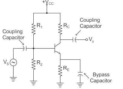
The advantage of the CE amplifier is its power gain will be high.
Coupling capacitors
These are used in an electronic circuit to pass the AC signal and blocks the unwanted DC components.
- The unwanted DC signals comes form the electronic devices or preceding stage of the electronic circuit.
- The reactive nature of the capacitor is useful for different behavior to different frequencies.
- In audio systems, DC sources are used to power audio circuits.
Coupling capacitors are essential components in amplifier circuits. They are used to prevent interference of a transistor’s bias voltage by AC signals.
In most amplifier circuits, this is achieved by driving the signal to the base terminal of a transistor through a coupling capacitor.
Conclusion:
Option C is correct.
A FET can be used as a variable- a)Inductor
- b)Capacitor
- c)Resistor
- d)Voltage Source
Correct answer is option 'C'. Can you explain this answer?
A FET can be used as a variable
a)
Inductor
b)
Capacitor
c)
Resistor
d)
Voltage Source
|
|
Pooja Patel answered |

- FET is a device that is usually operated in the constant-current portion of its output characteristics. But if it is operated on the region prior to pinch-off (that is where VDS is small, say below 100 mV), it will behave as a voltage-variable resistor.
- It is due to the fact that in this region drain-to-source resistance RDS can be controlled by varying the bias voltage VGS.
- In such applications the FET is also referred to as a voltage-variable resistor or volatile dependent resistor. It finds applications in many areas where this property is useful.
The drain of FET is analogous to BJT- a)collector
- b)emitter
- c)base
- d)drain
Correct answer is option 'A'. Can you explain this answer?
The drain of FET is analogous to BJT
a)
collector
b)
emitter
c)
base
d)
drain
|
|
Nilesh Joshi answered |
Analogies between FET and BJT
An analogy between Field Effect Transistor (FET) and Bipolar Junction Transistor (BJT) can be drawn in the context of their functioning. Both of these electronic devices are used for amplifying signals, and they have a similar structure in terms of the presence of a source, gate, and drain in FET and collector, base, and emitter in BJT. However, the way they function is different, and the analogy is drawn between the specific parts of the devices.
The drain of FET and collector of BJT
In FET, the drain is the part where the current flows out of the device. Similarly, in BJT, the collector is the part where the current flows out of the device. The analogy between these two parts is drawn based on their functionality. The collector in BJT is responsible for collecting the majority carriers (either electrons or holes) that flow from the emitter and then move towards the base. Similarly, the drain in FET is responsible for collecting the majority carriers that flow from the channel to the drain.
The analogy between the drain of FET and collector of BJT is further strengthened by the fact that both of these parts are operated in the reverse-biased mode. In BJT, the collector-base junction is reverse-biased, while in FET, the gate-source junction is reverse-biased. In both cases, the reverse-biasing results in a depletion region, which helps to control the flow of current through the device.
Conclusion
In conclusion, the analogy between the drain of FET and the collector of BJT is drawn based on their functionality and the way they operate in the device. Both of these parts are responsible for collecting the majority carriers and are operated in the reverse-biased mode. However, it is important to note that this analogy is limited to specific parts of the devices and does not imply that FET and BJT are the same.
Applications of negative feedback to a certain amplifier reduced its gain from 200 to 100. If the gain with the same feedback is to be raised to 150, in the case of another such appliance, the gain of the amplifier without feedback must have been- a)400
- b)450
- c)500
- d)600
Correct answer is option 'D'. Can you explain this answer?
Applications of negative feedback to a certain amplifier reduced its gain from 200 to 100. If the gain with the same feedback is to be raised to 150, in the case of another such appliance, the gain of the amplifier without feedback must have been
a)
400
b)
450
c)
500
d)
600
|
|
Hiral Kulkarni answered |
To understand why the gain of the amplifier without feedback must have been 600, we need to analyze the relationship between gain and negative feedback.
1. Gain reduction due to negative feedback:
When negative feedback is applied to an amplifier, it reduces the gain of the amplifier. In this case, the gain of the amplifier was reduced from 200 to 100.
2. Gain increase with feedback:
Now, we want to raise the gain with the same feedback to 150. This means that we need to increase the gain of the amplifier without feedback by a certain factor.
3. Relationship between gain with feedback and gain without feedback:
The gain with feedback (A_f) can be calculated using the following formula:
A_f = A / (1 + Aβ)
where A is the gain without feedback and β is the feedback factor.
4. Solving for the gain without feedback:
Given that the gain with feedback (A_f) is 150 and the gain with feedback (A) was previously 100, we can rearrange the formula to solve for the gain without feedback (A):
150 = A / (1 + Aβ)
150(1 + Aβ) = A
150 + 150Aβ = A
150Aβ - A = -150
A(150β - 1) = -150
A = -150 / (150β - 1)
5. Calculating the gain without feedback:
Now, we need to find the value of β that corresponds to the given gain reduction. The gain was reduced from 200 to 100, so the gain reduction is 200 - 100 = 100.
Using the formula for gain reduction due to negative feedback:
Gain reduction = A / (1 + Aβ) - A
100 = 200 / (1 + 200β) - 200
100(1 + 200β) = 200 - 200(1 + 200β)
100 + 20000β = 200 - 200 - 40000β
20000β + 40000β = 100
60000β = 100
β = 100 / 60000
β = 1/600
Substituting the value of β into the equation for A:
A = -150 / (150(1/600) - 1)
A = -150 / (1/4 - 1)
A = -150 / (-3/4)
A = 150 * 4/3
A = 200
6. Conclusion:
The gain without feedback (A) must have been 200 in order to achieve a gain of 150 with the given feedback. Therefore, the correct answer is option D) 600.
It is desired to reduce total harmonic of amplifier from 8% to 1% by use of 10% negative feedback. If the gain of the amplifier with original distortion and with reduced distortion is A1 and A2 then, A1 + A2 = −−−−−−
Correct answer is between '78.70,78.80'. Can you explain this answer?
It is desired to reduce total harmonic of amplifier from 8% to 1% by use of 10% negative feedback. If the gain of the amplifier with original distortion and with reduced distortion is A1 and A2 then, A1 + A2 = −−−−−−
|
|
Snehal Rane answered |
To solve this problem, we can use the formula for the reduction in distortion due to negative feedback:
Rd = 1 - (1 + β) * Hd
Where Rd is the reduction in distortion, β is the feedback factor, and Hd is the distortion without feedback.
Given that the reduction in distortion is desired to be from 8% to 1%, we can calculate the initial distortion without feedback (Hd) as:
Hd = 8% = 0.08
And the desired distortion with feedback (Hd') as:
Hd' = 1% = 0.01
We are also given that the feedback factor (β) is 10%.
Using the formula, we can calculate the reduction in distortion (Rd) as:
Rd = 1 - (1 + 0.1) * 0.08
= 1 - 1.08 * 0.08
= 1 - 0.0864
= 0.9136
Next, we can calculate the gain of the amplifier with reduced distortion (A2) using the formula:
A2 = A1 / (1 + β * A1 * Rd)
Where A1 is the gain of the amplifier with original distortion.
Since we want to find the relationship between A1 and A2, we can rearrange the formula to:
A2 = A1 / (1 + β * A1 * Rd)
A2 * (1 + β * A1 * Rd) = A1
A2 + β * A1 * Rd * A2 = A1
A2 - A1 = - β * A1 * Rd * A2
(A2 - A1) / (A1 * A2) = - β * Rd
(A2 - A1) / (A1 * A2 * Rd) = - β
Therefore, A1 * A2 = -(A2 - A1) / (β * Rd)
Substituting the values we have calculated:
A1 * A2 = -(A2 - A1) / (0.1 * 0.9136)
= -(A2 - A1) / 0.09136
An amplifier has a Open Loop voltage gain of –500. This gain is reduced to –100 when negative feedback is applied. The reverse transmission factor,β of this system is:-- a)– 0.025
- b)– 0.008
- c)0.1
- d)– 0.2
Correct answer is option 'B'. Can you explain this answer?
An amplifier has a Open Loop voltage gain of –500. This gain is reduced to –100 when negative feedback is applied. The reverse transmission factor,β of this system is:-
a)
– 0.025
b)
– 0.008
c)
0.1
d)
– 0.2
|
|
Pooja Patel answered |
Concept:
The gain of a feedback system is given by:

A = Open Loop gain
Af = Closed Loop Gain
β = Feedback/Transmission factor
Calculation:
Given Af = -100 and A = -500
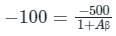
1 + Aβ = 5
Aβ = 4
β = 4 / -500 = -0.008
STC networks can be classified into two categories: low-pass (LP) and high-pass (HP). Then which of the following is true?- a)HP network passes dc and low frequencies and attenuate high frequency and opposite for LP network
- b)LP network passes dc and low frequencies and attenuate high frequency and opposite for HP network
- c)HP network passes dc and high frequencies and attenuate low frequency and opposite for LP network
- d)LP network passes low frequencies only and attenuate high frequency and opposite for HP network
Correct answer is option 'B'. Can you explain this answer?
STC networks can be classified into two categories: low-pass (LP) and high-pass (HP). Then which of the following is true?
a)
HP network passes dc and low frequencies and attenuate high frequency and opposite for LP network
b)
LP network passes dc and low frequencies and attenuate high frequency and opposite for HP network
c)
HP network passes dc and high frequencies and attenuate low frequency and opposite for LP network
d)
LP network passes low frequencies only and attenuate high frequency and opposite for HP network
|
|
Meghana Gupta answered |
Understanding Low-Pass and High-Pass Networks
Low-pass (LP) and high-pass (HP) networks are essential components in electrical engineering, particularly in signal processing. They are distinguished by their frequency response characteristics.
Low-Pass (LP) Networks
- Functionality: LP networks are designed to allow low frequencies to pass through while attenuating higher frequencies.
- DC Response: They pass direct current (DC) and low-frequency signals effectively.
- Frequency Attenuation: As the frequency increases beyond a certain cutoff point, the LP network reduces the signal amplitude significantly.
High-Pass (HP) Networks
- Functionality: HP networks do the opposite; they allow high frequencies to pass while attenuating low frequencies.
- DC Response: HP networks block DC (zero frequency) and low-frequency signals.
- Frequency Attenuation: Signals with frequencies below a specific cutoff frequency are significantly reduced in amplitude.
Explanation of Option B
- Correct Statement: Option B accurately states that LP networks pass DC and low frequencies while attenuating high frequencies, and the opposite holds true for HP networks.
- Comparison: This characterization aligns with the basic definitions of LP and HP filters in electrical engineering.
Conclusion
Understanding these characteristics is crucial for designing circuits that meet specific frequency requirements, ensuring optimal signal processing in various applications.
What will happen if values of Rs increase?- a)Vgs Increases
- b)Vgs Decreases
- c)Vgs Remains the same
- d)Vgs = 0
Correct answer is option 'B'. Can you explain this answer?
What will happen if values of Rs increase?
a)
Vgs Increases
b)
Vgs Decreases
c)
Vgs Remains the same
d)
Vgs = 0
|
|
Arindam Sengupta answered |
Introduction:
In this question, we are asked to determine the effect of increased values of resistance (Rs) on the voltage between the gate and source (Vgs) in a circuit. We are given four options to choose from, and the correct answer is option 'B' - Vgs decreases.
Explanation:
To understand why Vgs decreases when the resistance (Rs) increases, let's consider the basic operation of a field-effect transistor (FET).
Field-Effect Transistor (FET):
A field-effect transistor is a type of transistor that uses an electric field to control the flow of current. It has three terminals: the source (S), the drain (D), and the gate (G). The voltage between the gate and source (Vgs) determines the conductivity of the FET.
Effect of Rs on Vgs:
When the resistance (Rs) increases in a circuit, it means there is a higher voltage drop across Rs. This higher voltage drop reduces the voltage available at the source terminal of the FET. As a result, the voltage between the gate and source (Vgs) decreases.
Reasoning:
The reason for this decrease in Vgs can be understood by considering the voltage divider rule. The voltage divider rule states that the voltage across a resistor in a series circuit is proportional to its resistance value compared to the total resistance in the circuit.
In this case, Rs is in series with the source terminal of the FET. When Rs increases, it contributes a larger portion of the total resistance in the circuit. As a result, the voltage drop across Rs increases, causing a decrease in the voltage available at the source terminal.
Since Vgs is the voltage between the gate and source terminals, a decrease in the source voltage leads to a decrease in Vgs.
Conclusion:
In conclusion, when the resistance (Rs) increases in a circuit, the voltage between the gate and source (Vgs) of a field-effect transistor (FET) decreases. This can be explained by the voltage divider rule, where an increase in Rs leads to a higher voltage drop across it, reducing the voltage available at the source terminal and consequently decreasing Vgs.
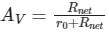
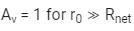
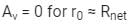
The ratio of the open circuit voltage of a voltage amplifier (AV) to the short circuit transconductance of a (Gm) of a transconductance amplifier, given that both have the same value of the internal resistance (Ri) and the output resistance (R0), is- a)Ri
- b)R0
- c)1/Ri
- d)1/R0
Correct answer is option 'B'. Can you explain this answer?
The ratio of the open circuit voltage of a voltage amplifier (AV) to the short circuit transconductance of a (Gm) of a transconductance amplifier, given that both have the same value of the internal resistance (Ri) and the output resistance (R0), is
a)
Ri
b)
R0
c)
1/Ri
d)
1/R0
|
|
Arya Mukherjee answered |
Understanding Voltage Amplifier and Transconductance Amplifier
The problem compares the open circuit voltage of a voltage amplifier (AV) with the short circuit transconductance (Gm) of a transconductance amplifier. To understand why the correct answer is R0, we need to delve into the definitions and relationships between these parameters.
Definitions
- **Open Circuit Voltage (AV)**: This is the output voltage of the voltage amplifier when the output is not loaded, meaning the load resistance is infinite.
- **Short Circuit Transconductance (Gm)**: This represents the output current per unit of input voltage change, measured when the output is shorted (i.e., output resistance is zero).
Relationship Between Parameters
1. **Internal Resistance (Ri)**:
- Both amplifiers have the same internal resistance, which affects how much of the input signal is transferred to the output.
2. **Output Resistance (R0)**:
- This is crucial in determining how the amplifier behaves under load. For the voltage amplifier, it can be seen as providing a certain voltage output when loaded.
Ratio Derivation
- The open circuit voltage for a voltage amplifier can be expressed as:
**AV = Vout / Vin**.
- The short circuit transconductance for a transconductance amplifier can be expressed as:
**Gm = Iout / Vin**.
- Since both amplifiers have the same output resistance (R0), the relationship between the output current and voltage can be simplified.
Conclusion
Thus, the ratio of open circuit voltage (AV) to short circuit transconductance (Gm) simplifies to the output resistance R0, leading to the final answer: **R0**. This indicates that under equivalent conditions, the output performance of both amplifiers is fundamentally tied to their output resistance.
Biasing is used in transition amplifiers to1. Stabilize the operating point against temperature variations.2. Place the operating point in the linear region of the characteristics.3. Make α, β and ICO of the transistor independent of temperature variations.4. Reduce distortion and increase dynamic range.- a)1, 2, 3 and 4
- b)1, 2 and 4 only
- c)1, 2 and 3 only
- d)2, 3 and 4 only
Correct answer is option 'B'. Can you explain this answer?
Biasing is used in transition amplifiers to
1. Stabilize the operating point against temperature variations.
2. Place the operating point in the linear region of the characteristics.
3. Make α, β and ICO of the transistor independent of temperature variations.
4. Reduce distortion and increase dynamic range.
a)
1, 2, 3 and 4
b)
1, 2 and 4 only
c)
1, 2 and 3 only
d)
2, 3 and 4 only
|
|
Pioneer Academy answered |
The purpose of Biasing in BJT amplifier:
i) To Stabilize Q-point in its linear region of operation (Q-point is an operating point).
[Statement 2 correct]
ii) To stabilize Q-point in against variation of temperature because
Ic = βIB + (1 + β) Ico
Ico → leakage current.
Where Ico, β1, and IB are temperature dependent.
i.e. Temp ↑ → Ico ↑ → β ↑ → α ↑
(∵β=α1−α)
[Statement 1 correct], [Statement 3 wrong]
iii) To reduce distortion and increase dynamic range.
Since biasing fixed the Q-point so that there is no variation in the output so distortion is reduced hence dynamic range i.e. operating range of the amplifier is improved.
[Statement 4 correct]
So, statement 1, 2, 4 are correct.
iv) Biasing must provide the operating point independent of β of the transistor. So that variation in β due to temperature change does not affect the Q-point of an amplifier.
Find the gate voltage for voltage divider having R1 = R2 = 1KΩ and VDD = 5V?- a)1V
- b)5V
- c)3V
- d)2.5V
Correct answer is option 'D'. Can you explain this answer?
Find the gate voltage for voltage divider having R1 = R2 = 1KΩ and VDD = 5V?
a)
1V
b)
5V
c)
3V
d)
2.5V
|
|
Raj Desai answered |
Given:
R1 = R2 = 1K (1 kiloohm)
VDD = 5V
To find:
Gate voltage (VG) for the voltage divider
Solution:
1. Voltage Divider Formula:
The voltage divider formula is given by:
VG = VDD * (R2 / (R1 + R2))
2. Substituting the given values:
VG = 5V * (1K / (1K + 1K))
= 5V * (1K / 2K)
= 5V * 0.5
= 2.5V
3. Answer:
The gate voltage for the voltage divider with R1 = R2 = 1K and VDD = 5V is 2.5V.
Therefore, the correct answer is option 'D' (2.5V).
Thermal runaway is not possible in FET because as the temperature increases - a)mobility decreases
- b)transconductance increases
- c)drain current increases
- d)none of these
Correct answer is option 'A'. Can you explain this answer?
Thermal runaway is not possible in FET because as the temperature increases
a)
mobility decreases
b)
transconductance increases
c)
drain current increases
d)
none of these
|
|
Pooja Patel answered |
Concept:
(1) The thermal runway is not possible in FET because as the temperature of the FET increases, the mobility decreases, i.e. if the Temperature (T) ↑, the carries Mobility (μn or μp) ↓, and Ips↓
(2) Since the current is decreasing with an increase in temperature, the power dissipation at the output terminal of a FET decreases or we can say that it’s minimum.
So, there will be no Question of thermal Runway at the output of the FET.
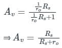
In a CD JFET configuration, if r0 = 1 / gm then:- a)
- b)

- c)
- d)
Correct answer is option 'A'. Can you explain this answer?
In a CD JFET configuration, if r0 = 1 / gm then:
a)
b)
c)
d)
|
|
Pooja Patel answered |
JFET common drain amplifier is sometimes considered as a source follower and has voltage gain less than unity.
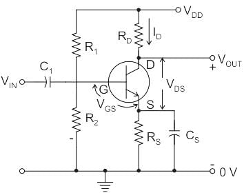
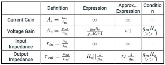
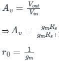
Putting the value of gm, we get
What is meant by stability of the an amplified signal?- a)The amplified signal must have a finite amplitude
- b)The amplified signal should not have self oscillation
- c)The input and the output signal must be proportional
- d)The ratio of the input and the output signal must be finite
Correct answer is option 'B'. Can you explain this answer?
What is meant by stability of the an amplified signal?
a)
The amplified signal must have a finite amplitude
b)
The amplified signal should not have self oscillation
c)
The input and the output signal must be proportional
d)
The ratio of the input and the output signal must be finite

|
Mahesh Yadav answered |
The ability of the amplifier to prevent self oscillation is a measure of its stability
Which factor determines the gain of the voltage series feedback amplifier?- a)Open loop voltage gain
- b)Feedback voltage
- c)Ratio of two resistors
- d)Gain of feedback circuit
Correct answer is option 'C'. Can you explain this answer?
Which factor determines the gain of the voltage series feedback amplifier?
a)
Open loop voltage gain
b)
Feedback voltage
c)
Ratio of two resistors
d)
Gain of feedback circuit
|
|
Tanvi Rane answered |
Understanding Voltage Series Feedback Amplifier Gain
The gain of a voltage series feedback amplifier is primarily influenced by the ratio of two resistors in the feedback network. Here's a detailed explanation:
Open Loop Voltage Gain
- Open loop voltage gain refers to the gain of the amplifier without any feedback applied. While it sets the initial gain level, it does not directly determine the final gain when feedback is employed.
Feedback Voltage
- Feedback voltage is the voltage returned from the output to the input of the amplifier. Although crucial for stability and linearity, it does not dictate the gain but rather regulates the output based on the feedback network.
Ratio of Two Resistors
- The key factor that determines the gain in a voltage series feedback amplifier is the ratio of two resistors in the feedback circuit. This resistance ratio sets the amount of feedback applied to the amplifier, thus controlling the overall gain.
- For instance, if resistors R1 and R2 are used in a feedback configuration, the gain can be expressed as A = R2/(R1 + R2). This equation shows that the gain is directly influenced by how these resistors are chosen.
Gain of Feedback Circuit
- The gain of the feedback circuit is an important consideration, but it is not the primary determinant of the overall amplifier gain. Instead, it works in conjunction with the resistor ratio to establish the final output.
Conclusion
In summary, while several factors contribute to the performance of a voltage series feedback amplifier, it is the ratio of two resistors that fundamentally determines its gain. Understanding this relationship is essential for designing effective feedback systems in electrical engineering.
Find the relative change in gain with negative feedback given that return ratio is 24, and feedback factor is 3, when the change in open loop gain is 2.- a)1
- b)1.6
- c)0.1
- d)0.01
Correct answer is option 'D'. Can you explain this answer?
Find the relative change in gain with negative feedback given that return ratio is 24, and feedback factor is 3, when the change in open loop gain is 2.
a)
1
b)
1.6
c)
0.1
d)
0.01
|
|
Vaibhav Joshi answered |
Solution:
Given data:
Return Ratio = 24
Feedback Factor = 3
Change in open loop gain = 2
Relative change in gain with negative feedback = ?
Formula used:
Relative change in gain with negative feedback = ΔA / (1 + Aβ)
Where,
ΔA = Change in open-loop gain
A = Open-loop gain
β = Feedback factor
Calculation:
From the given data, we know that
Return Ratio (R) = 1 / β
=> β = 1 / R
= 1 / 24
= 0.0417
Now, let's calculate the open-loop gain (A).
We know that A = R * (1 + β)
= 24 * (1 + 0.0417)
= 24.9992
The change in open-loop gain (ΔA) = 2
Using the formula, we can calculate the relative change in gain with negative feedback.
Relative change in gain with negative feedback = ΔA / (1 + Aβ)
= 2 / (1 + (24.9992 * 0.0417))
= 0.01
Therefore, the relative change in gain with negative feedback is 0.01.
Hence, the correct option is (d) 0.01.
General representation of the frequency response curve is called- a)Bode Plot
- b)Miller Plot
- c)Thevenin Plot
- d)Bandwidth Plot
Correct answer is option 'A'. Can you explain this answer?
General representation of the frequency response curve is called
a)
Bode Plot
b)
Miller Plot
c)
Thevenin Plot
d)
Bandwidth Plot

|
Sagnik Sen answered |
General representation of frequency response curves are called Bode plot. Bode plots are also called semi logarithmic plots since they have logarithmic values values on one of the axes.
Which of the following is true?- a)Coupling capacitors causes the gain to fall off at high frequencies
- b)Internal capacitor of a device causes the gain to fall off at low frequencies
- c)All of the mentioned
- d)None of the mentioned
Correct answer is option 'D'. Can you explain this answer?
Which of the following is true?
a)
Coupling capacitors causes the gain to fall off at high frequencies
b)
Internal capacitor of a device causes the gain to fall off at low frequencies
c)
All of the mentioned
d)
None of the mentioned
|
|
Rahul Chakraborty answered |
Internal Capacitors and Gain
Internal capacitors of a device do not cause the gain to fall off at low frequencies. In fact, internal capacitors are often used in electronic circuits to block DC voltage while allowing AC signals to pass through. They are designed to have a minimal impact on the gain of the circuit at low frequencies.
Coupling Capacitors and Gain
On the other hand, coupling capacitors are used to block DC components from one part of a circuit to another, allowing only the AC components to pass through. Coupling capacitors can cause the gain to fall off at high frequencies due to their impedance characteristics. As the frequency increases, the impedance of the coupling capacitor decreases, affecting the gain of the circuit at higher frequencies.
Conclusion
Therefore, the correct statement is that coupling capacitors cause the gain to fall off at high frequencies, not internal capacitors at low frequencies. It is crucial to understand the role of capacitors in a circuit to design and analyze electronic systems effectively.
When a circuit is called compensated attenuator?- a)Transfer function is directly proportional to the frequency
- b)Transfer function is inversely proportional to the frequency
- c)Transfer function is independent of the frequency
- d)Natural log of the transfer function is proportional to the frequency
Correct answer is option 'C'. Can you explain this answer?
When a circuit is called compensated attenuator?
a)
Transfer function is directly proportional to the frequency
b)
Transfer function is inversely proportional to the frequency
c)
Transfer function is independent of the frequency
d)
Natural log of the transfer function is proportional to the frequency

|
Atharva Rane answered |
Transfer function does not has frequency in its mathematical formula.
The common source stage of a CMOS amplifier Provides:- a)voltage gain, low i/p impedance and moderate o/p impedance
- b)Moderate voltage gain, high i/p impedance and high o/p impedance
- c)Moderate voltage gain, low i/p impedance and low o/p impedance
- d)Moderate voltage gain, high i/p impedance and moderate o/p impedance
Correct answer is option 'D'. Can you explain this answer?
The common source stage of a CMOS amplifier Provides:
a)
voltage gain, low i/p impedance and moderate o/p impedance
b)
Moderate voltage gain, high i/p impedance and high o/p impedance
c)
Moderate voltage gain, low i/p impedance and low o/p impedance
d)
Moderate voltage gain, high i/p impedance and moderate o/p impedance

|
Cstoppers Instructors answered |
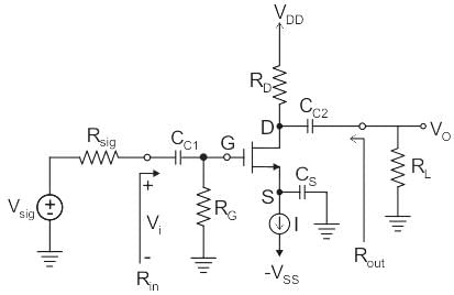
The value of Gate resistance (RG) is in mega-ohm (MΩ).
As Rin = RG
The input impedance of a common source amplifier is very high.
The value of ro, RD, and RL lies in kilo-ohm (kΩ). So the parallel combination of ro, RD, and RL is in kilo-ohm (kΩ). That’s why the output impedance and voltage gain of the common source amplifier is moderately high.
Ideal maximum voltage for common drain amplifier is _________- a)0
- b)1
- c)0.5
- d)2
Correct answer is option 'B'. Can you explain this answer?
Ideal maximum voltage for common drain amplifier is _________
a)
0
b)
1
c)
0.5
d)
2
|
|
Pooja Patel answered |
Similar to the transistor emitter follower, the source follower configuration itself provides a high level of buffering and a high input impedance. The actual input resistance of the FET itself is very high as it is a field effect device. This means that the source follower circuit is able to provide excellent performance as a buffer. The voltage gain is unity, although current gain is high. The input and output signals are in phase.
For a fixed bias circuit the drain current was 1mA, what is the value of source current?- a)0mA
- b)1mA
- c)2mA
- d)3mA
Correct answer is option 'C'. Can you explain this answer?
For a fixed bias circuit the drain current was 1mA, what is the value of source current?
a)
0mA
b)
1mA
c)
2mA
d)
3mA
|
|
Pooja Patel answered |
We know that for an FET same current flows through the gate and source terminal,
Hence source current=1mA.
Hence source current=1mA.
Consider a voltage amplifier having a frequency response of the low-pass STC type with a dc gain of 60 dB and a 3-dB frequency of 1000 Hz. Then the gain db at- a)f = 10 Hz is 55 db
- b)f = 10 kHz is 45 db
- c)f = 100 kHz is 25 db
- d)f = 1Mhz is 0 db
Correct answer is option 'D'. Can you explain this answer?
Consider a voltage amplifier having a frequency response of the low-pass STC type with a dc gain of 60 dB and a 3-dB frequency of 1000 Hz. Then the gain db at
a)
f = 10 Hz is 55 db
b)
f = 10 kHz is 45 db
c)
f = 100 kHz is 25 db
d)
f = 1Mhz is 0 db

|
Nandita Datta answered |
Use standard formulas for frequency response and voltage gain.
Which of the following is not a classification of amplifiers on the basis of their frequency response?- a)Capacitively coupled amplifier
- b)Direct coupled amplifier
- c)Bandpass amplifier
- d)None of the mentioned
Correct answer is option 'D'. Can you explain this answer?
Which of the following is not a classification of amplifiers on the basis of their frequency response?
a)
Capacitively coupled amplifier
b)
Direct coupled amplifier
c)
Bandpass amplifier
d)
None of the mentioned
|
|
Sanjana Chopra answered |
Classification of Amplifiers:
Amplifiers can be classified based on various criteria, including their frequency response. However, the classification of amplifiers based on frequency response does not include the option "None of the mentioned."
Explanation:
Capacitively Coupled Amplifier:
- A capacitively coupled amplifier is a type of amplifier that uses a capacitor to block DC signals while allowing AC signals to pass through. This helps in amplifying only the AC component of the input signal.
Direct Coupled Amplifier:
- A direct coupled amplifier is a type of amplifier that does not use any coupling capacitors in its circuit. This allows for amplification of both AC and DC components of the input signal.
Bandpass Amplifier:
- A bandpass amplifier is designed to amplify signals within a specific range of frequencies, known as the passband. It rejects signals outside this range, providing a band-limited amplification.
Conclusion:
- The classification of amplifiers based on their frequency response includes capacitively coupled amplifiers, direct coupled amplifiers, and bandpass amplifiers. The option "None of the mentioned" does not belong to this classification.
In order to prevent distortion in the output signal after amplification, the input signal must be- a)Higher than the positive saturation level of the amplifier
- b)Lower than the negative saturation level of the amplifier
- c)Must lie with the negative and the positive saturation level of the amplifier
- d)Both higher than the positive saturation level of the amplifier and lower than the negative saturation level of the amplifier
Correct answer is option 'C'. Can you explain this answer?
In order to prevent distortion in the output signal after amplification, the input signal must be
a)
Higher than the positive saturation level of the amplifier
b)
Lower than the negative saturation level of the amplifier
c)
Must lie with the negative and the positive saturation level of the amplifier
d)
Both higher than the positive saturation level of the amplifier and lower than the negative saturation level of the amplifier

|
Mrinalini Sen answered |
Higher than the positive saturation and lower than the negative saturation level of the amplifier are the desired characteristics in order to prevent distortion.
The negative feedback in an amplifier leads to which one of the following?- a)Increase in current gain
- b)Increase in voltage gain
- c)Decrease in voltage gain
- d)Decrease in bandwidth
Correct answer is option 'C'. Can you explain this answer?
The negative feedback in an amplifier leads to which one of the following?
a)
Increase in current gain
b)
Increase in voltage gain
c)
Decrease in voltage gain
d)
Decrease in bandwidth
|
|
Pooja Patel answered |
The negative feedback in amplifiers causes:
- Reduced the gain and increases the stability in G.
- Increases the bandwidth to maintain constant gain-bandwidth product
- Reduces the distortion and noise in the amplifier
- The signal-to-noise ratio is not affected.
- The voltage gain (Av) of an amplifier is defined as the ratio of output voltage to the input voltage.
Av = Vo/Vin
Here, Vo is the output voltage of an amplifier and Vin is the input voltage of an amplifier.
- In a negative feedback amplifier, closed-loop voltage gain is given
Av = Vo / Vin = 1/(1+Aoβ)
Here, β = feedback factor,
Ao = open-loop gain of the amplifier.
- This expression clearly shows that closed-loop voltage gain has reduced by introducing negative feedback.
- We know that a product of gain and bandwidth is inversely proportional so here bandwidth of amplifier will increase ;
(gain × bandwidth = 0.35)
- A negative feedback amplifier decreases the current gain.
The bandwidth of an RC-coupled amplifier is limited by- a)Coupling capacitors at the low frequency end and bypass capacitors at the high frequency end
- b)Coupling capacitors at the high frequency end and bypass capacitors at the low frequency end
- c)Bypass and coupling capacitors at the low frequency end and device shunt capacitors at the high frequency end
- d)Device shunt capacitors at the low frequency end and bypass as well as coupling capacitors at the high frequency end
Correct answer is option 'C'. Can you explain this answer?
The bandwidth of an RC-coupled amplifier is limited by
a)
Coupling capacitors at the low frequency end and bypass capacitors at the high frequency end
b)
Coupling capacitors at the high frequency end and bypass capacitors at the low frequency end
c)
Bypass and coupling capacitors at the low frequency end and device shunt capacitors at the high frequency end
d)
Device shunt capacitors at the low frequency end and bypass as well as coupling capacitors at the high frequency end
|
|
Pooja Patel answered |
(i) In capacitively coupled amplifiers, the coupling and bypass capacitors affect the low-frequency cut-off. These capacitors form a high-pass filter with circuit resistances.
(ii) Coupling and bypass capacitors are also called external capacitors.
For high-frequency response, it is determined by the device’s internal capacitance and the Miller effect.
(iii) Device internal capacitance is shunted and also called as Junction capacitors.
(ii) Coupling and bypass capacitors are also called external capacitors.
For high-frequency response, it is determined by the device’s internal capacitance and the Miller effect.
(iii) Device internal capacitance is shunted and also called as Junction capacitors.
Which among the following is not a special case of voltage shut feedback amplifier?- a)Voltage follower
- b)Current to voltage connector
- c)Inverter
- d)None of the mentioned
Correct answer is option 'A'. Can you explain this answer?
Which among the following is not a special case of voltage shut feedback amplifier?
a)
Voltage follower
b)
Current to voltage connector
c)
Inverter
d)
None of the mentioned
|
|
Ameya Gupta answered |
Introduction:
In voltage shut feedback amplifiers, the output voltage is fed back to the input in such a way that it opposes any change in the input voltage. This feedback mechanism is used to stabilize and control the gain of the amplifier. There are various special cases of voltage shut feedback amplifiers, each with its own characteristics and applications.
Voltage Follower:
A voltage follower, also known as a unity gain amplifier or a buffer, is a special case of voltage shut feedback amplifier. In a voltage follower, the output voltage follows the input voltage, hence the name. The voltage gain of a voltage follower is unity, which means the output voltage is the same as the input voltage.
Current to Voltage Converter:
A current to voltage converter, also known as a transimpedance amplifier, is another special case of voltage shut feedback amplifier. It converts an input current into an output voltage. The output voltage is proportional to the input current, and the proportionality constant is determined by the feedback resistor.
Inverter:
An inverter, also known as an inverting amplifier, is a special case of voltage shut feedback amplifier where the output voltage is the inverse of the input voltage. The inverter has a negative voltage gain, which means it amplifies the input voltage with an opposite polarity. The voltage gain is determined by the feedback resistor and the input resistor.
Explanation:
The correct answer is option 'A', voltage follower. A voltage follower is not a special case of voltage shut feedback amplifier. It is a basic amplifier configuration where the output voltage is directly connected to the input. There is no feedback mechanism involved in a voltage follower, and the gain is unity. It is mainly used to isolate the input signal from the load and provide high input impedance.
Conclusion:
In summary, the special cases of voltage shut feedback amplifiers include voltage follower, current to voltage converter, and inverter. These configurations have different characteristics and applications. The voltage follower is not a special case of voltage shut feedback amplifier as it does not involve any feedback mechanism.
An amplifier has a voltage gain of 40db. The value of AVO is- a)10
- b)100
- c)20
- d)200
Correct answer is option 'B'. Can you explain this answer?
An amplifier has a voltage gain of 40db. The value of AVO is
a)
10
b)
100
c)
20
d)
200

|
Jaya Yadav answered |
The expression is given by 10 log AVO = 40. Solving for Avo gives 100 as the answer.
The voltage gain of a common-source JFET amplifier depends up on its- a)Input impedance
- b)Amplification factor
- c)Dynamic drain resistance
- d)Drain load resistance
Correct answer is option 'D'. Can you explain this answer?
The voltage gain of a common-source JFET amplifier depends up on its
a)
Input impedance
b)
Amplification factor
c)
Dynamic drain resistance
d)
Drain load resistance
|
|
Mainak Pillai answered |
Explanation:
A JFET (Junction Field Effect Transistor) is a type of transistor that uses an electric field to control the conductivity of a channel in a semiconductor material. Common-source JFET amplifiers are used in audio and voltage amplifier circuits.
Voltage gain refers to the ratio of output voltage to input voltage in an amplifier circuit. The voltage gain of a common-source JFET amplifier depends on several factors, including:
1. Drain load resistance: The drain load resistance is the resistance connected between the drain of the JFET and the power supply. The higher the value of the drain load resistance, the higher the voltage gain of the amplifier.
2. Input impedance: The input impedance is the resistance seen by the input signal source. The higher the input impedance of the amplifier, the higher the voltage gain.
3. Amplification factor: The amplification factor is the ratio of the change in drain current to the change in gate-source voltage. The higher the amplification factor of the JFET, the higher the voltage gain of the amplifier.
4. Dynamic drain resistance: The dynamic drain resistance is the resistance seen by the drain of the JFET when the gate-source voltage is varied. The higher the dynamic drain resistance, the higher the voltage gain of the amplifier.
Out of the above factors, drain load resistance has the most significant effect on voltage gain, as it directly affects the output voltage of the amplifier. Hence, option D (Drain load resistance) is the correct answer.
Which of the following isn’t true?- a)Both transformer and amplifier can provide voltage gain
- b)Both transformer and amplifier can provide current gain
- c)Both transformer and amplifier can provide power gain
- d)None of the mentioned
Correct answer is option 'C'. Can you explain this answer?
Which of the following isn’t true?
a)
Both transformer and amplifier can provide voltage gain
b)
Both transformer and amplifier can provide current gain
c)
Both transformer and amplifier can provide power gain
d)
None of the mentioned

|
Ankit Mukherjee answered |
For an ideal transformer the power input is always equal to the power output. In real conditions there is slight loss of power when transferring the power from an input source to an output source. Amplifiers only provide power gain.
If a certain drain JFET has a transconductance of 4ms. And has external drain resistance of 1.5 ohm than ideal voltage gain will be _________- a)4
- b)5
- c)6
- d)8
Correct answer is option 'C'. Can you explain this answer?
If a certain drain JFET has a transconductance of 4ms. And has external drain resistance of 1.5 ohm than ideal voltage gain will be _________
a)
4
b)
5
c)
6
d)
8
|
|
Nandita Bajaj answered |
Given data:
- Transconductance (gm) of the JFET = 4 ms
- External drain resistance (RD) = 1.5 ohm
We need to find the ideal voltage gain.
The ideal voltage gain (Av) of a JFET amplifier can be calculated using the formula:
Av = -gm * RD
Explanation:
1. Transconductance (gm):
The transconductance (gm) is a measure of how much the drain current (ID) changes for a given change in the gate-source voltage (VGS).
It is given by the formula:
gm = ΔID / ΔVGS
Here, gm is in siemens (S), ID is in amperes (A), and VGS is in volts (V).
2. External drain resistance (RD):
The external drain resistance (RD) is the resistance connected to the drain terminal of the JFET. It is used to provide the load for the amplifier.
3. Ideal voltage gain (Av):
The ideal voltage gain (Av) is the ratio of the change in output voltage (ΔVout) to the change in input voltage (ΔVin) in the amplifier.
It can be calculated using the formula:
Av = ΔVout / ΔVin
In a JFET amplifier, the ideal voltage gain is given by:
Av = -gm * RD
Explanation of the formula:
- The negative sign in the formula is due to the fact that the JFET is a voltage-controlled device and the output voltage is out of phase with the input voltage.
- The transconductance (gm) determines the slope of the transfer characteristic curve of the JFET.
- The external drain resistance (RD) determines the load on the JFET and thus affects the gain.
In this case, the transconductance (gm) is given as 4 ms and the external drain resistance (RD) is given as 1.5 ohm.
Therefore, the ideal voltage gain (Av) can be calculated as:
Av = -4 ms * 1.5 ohm = -6
The negative sign indicates that the output voltage will be out of phase with the input voltage.
Hence, the ideal voltage gain is 6 (option C).
A common gate amplifier has- a)high input resistance and high output resistance
- b)low input resistance and high output resistance
- c)low input resistance and low output resistance
- d)high input resistance and low output resistance
Correct answer is option 'B'. Can you explain this answer?
A common gate amplifier has
a)
high input resistance and high output resistance
b)
low input resistance and high output resistance
c)
low input resistance and low output resistance
d)
high input resistance and low output resistance
|
|
Pooja Patel answered |
FET:
As the input circuit of FET is reverse biased, FET exhibits a much higher input impedance ( in the order of 100 M 12 ) and lower output impedance and there will be a high degree of isolation between input and output.
So, FET can act as an excellent buffer amplifier but the BJT has low input impedance because its input circuit is forward biased.
Buffer amplifier needs to have- a)Low input resistance and low output resistance
- b)High Input resistance and high output resistance
- c)Low input resistance and high output resistance
- d)High input resistance and low output resistance
Correct answer is option 'D'. Can you explain this answer?
Buffer amplifier needs to have
a)
Low input resistance and low output resistance
b)
High Input resistance and high output resistance
c)
Low input resistance and high output resistance
d)
High input resistance and low output resistance

|
Bibek Mukherjee answered |
Buffer amplifiers are used to connect high input resistance source to a low output resistance load.
Single-time-constant (STC) networks are those networks that are composed of, or can be reduced to- a)One reactive component (L or C) and a resistance (R)
- b)Only capacitive component (C) and resistance (R)
- c)Only inductive component (L) and resistance (R)
- d)Reactive components (L, C or both L and C) and resistance (R)
Correct answer is option 'A'. Can you explain this answer?
Single-time-constant (STC) networks are those networks that are composed of, or can be reduced to
a)
One reactive component (L or C) and a resistance (R)
b)
Only capacitive component (C) and resistance (R)
c)
Only inductive component (L) and resistance (R)
d)
Reactive components (L, C or both L and C) and resistance (R)

|
Charvi Kaur answered |
STC has only one reactive component and one resistive component.
The most commonly used feedback arrangement in cascaded amplifier is:- a)current shunt feedback
- b)frequency series feedback
- c)voltage shunt feedback
- d)voltage series feedback
Correct answer is option 'D'. Can you explain this answer?
The most commonly used feedback arrangement in cascaded amplifier is:
a)
current shunt feedback
b)
frequency series feedback
c)
voltage shunt feedback
d)
voltage series feedback
|
|
Cstoppers Instructors answered |
Analysis:-
Voltage series feedback is the most commonly used feedback arrangement in cascaded amplifiers.
This configuration increases input resistance and decreases output resistance.

Benefit of high input impedance:
- It provides good amplification to the input signal, otherwise, we get low voltage and that leads to low amplification.
- It minimizes the loading effect on input and a thus significant amount of input voltage signal is maintained for amplification.
Chapter doubts & questions for Amplifiers - Electrical Engineering Optional Notes for UPSC 2025 is part of UPSC CSE exam preparation. The chapters have been prepared according to the UPSC CSE exam syllabus. The Chapter doubts & questions, notes, tests & MCQs are made for UPSC CSE 2025 Exam. Find important definitions, questions, notes, meanings, examples, exercises, MCQs and online tests here.
Chapter doubts & questions of Amplifiers - Electrical Engineering Optional Notes for UPSC in English & Hindi are available as part of UPSC CSE exam.
Download more important topics, notes, lectures and mock test series for UPSC CSE Exam by signing up for free.
Electrical Engineering Optional Notes for UPSC
550 videos|588 docs|343 tests
|
|
© EduRev
|
Education Revolution
|


|


Signup to see your scores
go up within 7 days!
Access 1000+ FREE Docs, Videos and Tests
Takes less than 10 seconds to signup