All Exams >
GATE Physics >
Electronics for GATE >
All Questions
All questions of Bipolar Junction Transistors for GATE Physics Exam
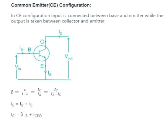
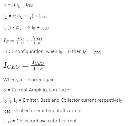
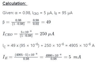
A npn transistor circuit has ∝ = 0.985. If IC = 2mA then the value of lB (in mA) is?
Correct answer is '0.03'. Can you explain this answer?
A npn transistor circuit has ∝ = 0.985. If IC = 2mA then the value of lB (in mA) is?
|
|
Vedika Singh answered |
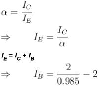
= 0.03 mA
The correct answer is: 0.03
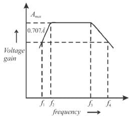
The frequency response curve of a RC coupled amplifier is shown in the given diagram.Based on it, what is the bandwidth?
- a)

- b)

- c)

- d)

Correct answer is option 'D'. Can you explain this answer?
The frequency response curve of a RC coupled amplifier is shown in the given diagram.Based on it, what is the bandwidth?


a)

b)

c)

d)

|
|
Vedika Singh answered |
The difference of frequencies when amplitude becomes 70% of maximum is called as bandwidth.
Hence, bandwidth =
The correct answer is:
Hence, bandwidth =

The correct answer is:

Which of the following are true in case of negative feedback amplifiers. - a)Bandwidth of the amplifier decreases
- b)Stability of the amplifier decreases
- c)Noise of the amplifier decreases
- d)Distortion of the amplifier decreases
Correct answer is option 'A,C,D'. Can you explain this answer?
Which of the following are true in case of negative feedback amplifiers.
a)
Bandwidth of the amplifier decreases
b)
Stability of the amplifier decreases
c)
Noise of the amplifier decreases
d)
Distortion of the amplifier decreases

|
Pie Academy answered |
Negative feedback amplifiers are specifically designed to improve the stability of the amplifier, decrease the distortion of the amplifiers, noise in the amplifier and bandwidth of the amplifier.
The correct answers are: Distortion of the amplifier decreases, Noise of the amplifier decreases, Bandwidth of the amplifier decreases
The correct answers are: Distortion of the amplifier decreases, Noise of the amplifier decreases, Bandwidth of the amplifier decreases
A common emitter transistor amplifier circuit is operated under a fixed bias. In this circuit, the operating point.- a)moves towards the saturation region with an increase in temperature
- b)moves towards the saturation region with a decrease in temperature
- c)remains fixed with an increase in temperature
- d)moves toward cut-off region with an increase in temperature
Correct answer is option 'B'. Can you explain this answer?
A common emitter transistor amplifier circuit is operated under a fixed bias. In this circuit, the operating point.
a)
moves towards the saturation region with an increase in temperature
b)
moves towards the saturation region with a decrease in temperature
c)
remains fixed with an increase in temperature
d)
moves toward cut-off region with an increase in temperature

|
Pie Academy answered |
The common emitter circuit configuration provides voltage gain combined with a moderate current gain, as well as a medium input and a medium output impedance. As such the common emitter configuration is a good all round circuit for use in many applications.
It is also worth noting at this stage that the common emitter transistor amplifier inverts the signal at the input. Therefore if a waveform that is rising enters the input of the common emitter amplifier, it will cause the output voltage to fall. In other words it has a 180° phase change across the circuit.
Dependent upon the actual electronic circuit design itself, the common emitter does not use too many electronic components, sometimes as few as two resistors, although if the bias needs setting for analogue circuits, then four resistors and three capacitors may be used.
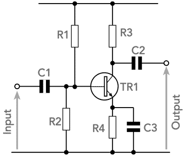
In fixed bias, when temperature is increased, the operating point moves toward the saturation region.
The correct answer is: moves towards the saturation region with a decrease in temperature
The correct answer is: moves towards the saturation region with a decrease in temperature
Choose the following options in respect of a BJT connected in the common-emitter configuration.- a)Voltage gain is medium
- b)Low input impedance
- c)Low Power gain
- d)Highest power gain
Correct answer is option 'A,B,D'. Can you explain this answer?
Choose the following options in respect of a BJT connected in the common-emitter configuration.
a)
Voltage gain is medium
b)
Low input impedance
c)
Low Power gain
d)
Highest power gain
|
|
Jayant Mishra answered |
If BJT connected in common emitter configurations, the power gain is highest, voltage gain is medium, input impedence is low.
The correct answers are: Voltage gain is medium, Low input impedance , Highest power gain
The correct answers are: Voltage gain is medium, Low input impedance , Highest power gain
Consider the following statements about an oscillator and choose which of them are true. An oscillator- a)has noise as the initial signal
- b)consists of a noise injecting network
- c)consists of a frequency selecting network
- d)consists of a positive feedback amplifier
Correct answer is option 'A,C,D'. Can you explain this answer?
Consider the following statements about an oscillator and choose which of them are true. An oscillator
a)
has noise as the initial signal
b)
consists of a noise injecting network
c)
consists of a frequency selecting network
d)
consists of a positive feedback amplifier
|
|
Jayant Mishra answered |
An oscillator is a system consisting of active and passive circuit elements to produce a sinusoidal or other respective waveforms at the output without the amplification of an external source (signal). It transforms the dc power from the source to the ac power in the load.
This consists of a positive feedback amplifier and has noise as the initial signal and consists of a frequency signal selector.
The correct answers are: consists of a positive feedback amplifier, has noise as the initial signal, consists of a frequency selecting network
This consists of a positive feedback amplifier and has noise as the initial signal and consists of a frequency signal selector.
The correct answers are: consists of a positive feedback amplifier, has noise as the initial signal, consists of a frequency selecting network
A common emitter amplifier has voltage gain of 50, an input impedance of 1000Ω and an output impedance of 200Ω. The power gain of the amplifier will be (in dB).
Correct answer is '250'. Can you explain this answer?
A common emitter amplifier has voltage gain of 50, an input impedance of 1000Ω and an output impedance of 200Ω. The power gain of the amplifier will be (in dB).
|
|
Vedika Singh answered |
Power gain = Voltage gain x current gain

The correct answer is: 250

The correct answer is: 250
Which of the following are essential for maintaining oscillations in an oscillator ?- a)Design of load (phase shifting network)
- b)Positive feedback
- c)Non-linear biasing circuit
- d)High gain amplifier
Correct answer is option 'A,B,C,D'. Can you explain this answer?
Which of the following are essential for maintaining oscillations in an oscillator ?
a)
Design of load (phase shifting network)
b)
Positive feedback
c)
Non-linear biasing circuit
d)
High gain amplifier
|
|
Jayant Mishra answered |
For maintaining oscillation in an oscillator, all the four options above are required which are positive feedback, phase shifting network, non-linear biasing circuit and high gain amplifier. Without any one of the above, we will not obtain a sustained oscillation in an oscillator.
The correct answers are: Positive feedback, Design of load (phase shifting network), Non-linear biasing circuit, High gain amplifier
The correct answers are: Positive feedback, Design of load (phase shifting network), Non-linear biasing circuit, High gain amplifier
At very high frequency, mica capacitor are used, because.
- a)of low ohmic losses and less reactance.
- b)leakage loss in mica exist
- c)the additional energy for reversal of dielectric in ac field is small
- d)the retention of charge by mica is negligible
Correct answer is option 'A'. Can you explain this answer?
At very high frequency, mica capacitor are used, because.
a)
of low ohmic losses and less reactance.
b)
leakage loss in mica exist
c)
the additional energy for reversal of dielectric in ac field is small
d)
the retention of charge by mica is negligible
|
|
Jayant Mishra answered |
Mica capacitors are preferred for high frequency circuits because they have low ohmic losses and less reactance.
A pnp transistor can be considered to be equivalent to two diodes as shown in figure.- a)

- b)

- c)

- d)

Correct answer is option 'A'. Can you explain this answer?
A pnp transistor can be considered to be equivalent to two diodes as shown in figure.
a)

b)

c)

d)

|
|
Vedika Singh answered |

The direction of current is always from p to n.
The correct answer is:

For a BJT, the current amplification factor ∝ = 0.9 . This transistor is connected in common emitter configurations. When the base current changes by 0.4 mA, the change in collector current will be (in mA).
Correct answer is '3.6'. Can you explain this answer?
For a BJT, the current amplification factor ∝ = 0.9 . This transistor is connected in common emitter configurations. When the base current changes by 0.4 mA, the change in collector current will be (in mA).
|
|
Jayant Mishra answered |
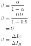

The correct answer is: 3.6
In common emitter mode, the input characteristics of a BJT is the variation of :- a)lB versus VCE at Constant VBE
- b)lC versus VCE at Constant VBE
- c)lC versus VCE at Constant IBE
- d)lB versus VBE at Constant VCE
Correct answer is option 'D'. Can you explain this answer?
In common emitter mode, the input characteristics of a BJT is the variation of :
a)
lB versus VCE at Constant VBE
b)
lC versus VCE at Constant VBE
c)
lC versus VCE at Constant IBE
d)
lB versus VBE at Constant VCE
|
|
Jayant Mishra answered |
In common emitter mode, lE = lB + lC
The input characteristics of the transistor represents the variation of base current lB with base emitter voltage VBE keeping VCE fixed.
The correct answer is: lB versus VBE at Constant VCE
The input characteristics of the transistor represents the variation of base current lB with base emitter voltage VBE keeping VCE fixed.
The correct answer is: lB versus VBE at Constant VCE
Which of the following is true for the active region of an NPN transistor?
- a)The collector current is inversely proportional to the base current
- b)The potential difference between the emitter and the collector is less than 0.1 V
- c)The collector current is directly proportional to the base current
- d)None of the mentioned
Correct answer is option 'C'. Can you explain this answer?
Which of the following is true for the active region of an NPN transistor?
a)
The collector current is inversely proportional to the base current
b)
The potential difference between the emitter and the collector is less than 0.1 V
c)
The collector current is directly proportional to the base current
d)
None of the mentioned
|
|
Vedika Singh answered |

The dc load line of an amplifier circuit.- a)contains the Q - point
- b)has a curvature
- c)has a positive slope
- d)has a negative slope
Correct answer is option 'A,D'. Can you explain this answer?
The dc load line of an amplifier circuit.
a)
contains the Q - point
b)
has a curvature
c)
has a positive slope
d)
has a negative slope
|
|
Jayant Mishra answered |
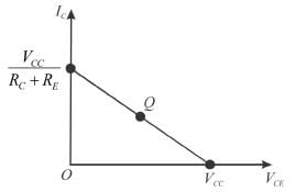
The dc load line has a negative slope and Q-point lies on this line.
The correct answers are: contains the Q - point, has a negative slope
Which one of the following is correct for a common base configuration of a transistor? - a)low input resistance, high output resistance
- b)low current gain, low input resistance
- c)low voltage gain, high current gain
- d)high voltage gain, low output resistance
Correct answer is option 'D'. Can you explain this answer?
Which one of the following is correct for a common base configuration of a transistor?
a)
low input resistance, high output resistance
b)
low current gain, low input resistance
c)
low voltage gain, high current gain
d)
high voltage gain, low output resistance
|
|
Jayant Mishra answered |
Any common base configuration of a transistor generally has very high voltage gain and low output resistance.
The correct answer is: high voltage gain, low output resistance
The correct answer is: high voltage gain, low output resistance
A transistor is used to make a common-base amplifier. If the transistor is npn and when it is biased in the active region, choose the correct option of the following.- a)Emitter and collector are both forward biased
- b)Emitter is reverse biased and collector is forward biased
- c)Emitter is forward biased and collector is reverse biased
- d)Emitter and collector are both reverse biased
Correct answer is option 'C'. Can you explain this answer?
A transistor is used to make a common-base amplifier. If the transistor is npn and when it is biased in the active region, choose the correct option of the following.
a)
Emitter and collector are both forward biased
b)
Emitter is reverse biased and collector is forward biased
c)
Emitter is forward biased and collector is reverse biased
d)
Emitter and collector are both reverse biased
|
|
Jayant Mishra answered |
For an npn common base amplifier, emitter is always forward biased and collector is reverse biased.
The correct answer is: Emitter is forward biased and collector is reverse biased
The correct answer is: Emitter is forward biased and collector is reverse biased
Which one of the following statements is true for a semiconductor p - n junction with no-external bias?- a)The p-side of the junction is negatively charged
- b)No charge develops anywhere in the junction
- c)The p-side of the junction is positively charged
- d)The total charge in the junction is not conserved
Correct answer is option 'A'. Can you explain this answer?
Which one of the following statements is true for a semiconductor p - n junction with no-external bias?
a)
The p-side of the junction is negatively charged
b)
No charge develops anywhere in the junction
c)
The p-side of the junction is positively charged
d)
The total charge in the junction is not conserved
|
|
Jayant Mishra answered |
The region containing the uncomposed acceptor and and donor ions is called depletion region i.e., there is a depletion of mobile charge (holes and free electrons) in this region. Since, this region has immobile ions which are electrically charge, it is also referred to as the space charge region. The electrical field between the acceptor and the donor ions is called a barrier. It is clear that p-side of the junction is negatively charged.
The correct answer is: The p-side of the junction is negatively charged
The correct answer is: The p-side of the junction is negatively charged
A crystal oscillator provides a very stable frequency because of.- a)high stability of the crystal
- b)low
 ratio of the crystal
 - c)high Q of the crystal
- d)the rigid crystal structure
Correct answer is option 'C'. Can you explain this answer?
A crystal oscillator provides a very stable frequency because of.
a)
high stability of the crystal
b)
low  ratio of the crystal
 ratio of the crystal
c)
high Q of the crystal
d)
the rigid crystal structure
|
|
Jayant Mishra answered |
Sharpness is the measurement of the stability. Sharpness increases means durability increases, since sharpness is directly proportional to quality factor Q. Hence, a crystal oscillator provides stable frequency because of high Q of the crystal.
The correct answer is: high Q of the crystal
The correct answer is: high Q of the crystal
Calculate VCE in the figure (in volts).
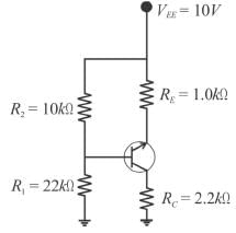
Correct answer is '2.26'. Can you explain this answer?
Calculate VCE in the figure (in volts).


|
|
Arghya answered |
First check to see if Rin (Base) can be neglected.

=150 x kΩ = 150kΩ
Since 150kΩ is more than 10 times R2. The condition is met and Rin(base) can be neglected.
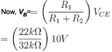
= 6.88 V
Then, VE = VB + VBE
= 6.88 + 0.7
VE = 7.58V
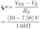
lE = 2.42 mA
From IE we can determine lc and VCE

and VC = ICRC = 2.42 mA x 2.2kΩ
= 5.32

= 2.26V
The correct answer is: 2.26

=150 x kΩ = 150kΩ
Since 150kΩ is more than 10 times R2. The condition
 is met and Rin(base) can be neglected.
= 6.88 V
Then, VE = VB + VBE
= 6.88 + 0.7
VE = 7.58V

lE = 2.42 mA
From IE we can determine lc and VCE

and VC = ICRC = 2.42 mA x 2.2kΩ
= 5.32

= 2.26V
The correct answer is: 2.26
In a typical npn transistor, the doping concentrations in emitter, base and collector regions are nE, nB, nC respectively. These satisfy the relation.- a)

- b)

- c)

- d)

Correct answer is option 'D'. Can you explain this answer?
In a typical npn transistor, the doping concentrations in emitter, base and collector regions are nE, nB, nC respectively. These satisfy the relation.
a)

b)

c)

d)

|
|
Jayant Mishra answered |
In an npn transistor, emitter heavily doped, collector is moderately doped and base very thin and least doped, i.e.

The correct answer is:

The correct answer is:

If a sinusoidal voltage is applied to the base of a biased npn transistor and resulting sinusoidal collector voltage is clipped near zero volts, the transistor is.- a)being driven into saturation
- b)being driven into cut-off
- c)operating non-linearly
- d)none of these
Correct answer is option 'A,C'. Can you explain this answer?
If a sinusoidal voltage is applied to the base of a biased npn transistor and resulting sinusoidal collector voltage is clipped near zero volts, the transistor is.
a)
being driven into saturation
b)
being driven into cut-off
c)
operating non-linearly
d)
none of these
|
|
Jayant Mishra answered |
Here, the transistor is being driven into saturation which is also a non-linear response. The transistor will not be driven into the cut-off region.
The correct answers are: being driven into stauration, operating non-linearly
The correct answers are: being driven into stauration, operating non-linearly
A power amplifier gives 150 W output of or an input of 1.5W. The gain in dB is :
Correct answer is '40'. Can you explain this answer?
A power amplifier gives 150 W output of or an input of 1.5W. The gain in dB is :
|
|
Vedika Singh answered |

= 40 dB
The correct answer is: 40
If the transistor amplifier has a gain of 20dB, then the ratio of output to input power is :
Correct answer is '100'. Can you explain this answer?
If the transistor amplifier has a gain of 20dB, then the ratio of output to input power is :
|
|
Vedika Singh answered |
The ratio of output to input power is known as power amplification.

The logarithm of the power amplification is represented in bel.
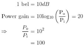
he correct answer is: 100

The logarithm of the power amplification is represented in bel.

he correct answer is: 100
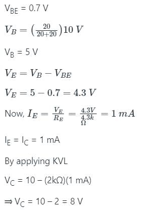
For a transistor circuit, VCE when Vin = 0V (in volts).
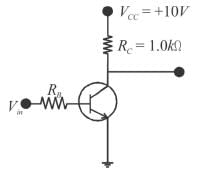
Correct answer is '10'. Can you explain this answer?
For a transistor circuit, VCE when Vin = 0V (in volts).


|
|
Jayant Mishra answered |
When Vin = 0V, the transistor is in cut-off (acts like an open switch) and VCE =VCC = 10V.
The correct answer is: 10
The correct answer is: 10
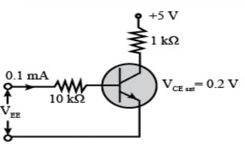
In the following circuit, Tr1 and Tr2 are identical transistors having VBE = 0.7V. The current passing through the transistor Tr2 is (in mA).
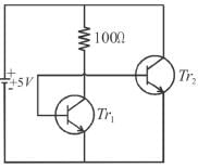
Correct answer is '43'. Can you explain this answer?
In the following circuit, Tr1 and Tr2 are identical transistors having VBE = 0.7V. The current passing through the transistor Tr2 is (in mA).


|
|
Jayant Mishra answered |
Applying KVL,
5=100x1 + 0.7

The correct answer is: 43
5=100x1 + 0.7

The correct answer is: 43
An electronic oscillator gives sustained oscillations when the feedback is.- a)in phase with the input
- b)negative
- c)positive
- d)out of phase with input
Correct answer is option 'A,B'. Can you explain this answer?
An electronic oscillator gives sustained oscillations when the feedback is.
a)
in phase with the input
b)
negative
c)
positive
d)
out of phase with input
|
|
Jayant Mishra answered |
An electronic oscillator gives sustained oscillations when the feedback is negative and in phase with the input.
The correct answers are: negative, in phase with the input
The correct answers are: negative, in phase with the input
An amplifier of gain 1000 is made into a feedback amplifier by feeding 9.9% of its output voltage in series with the input opposing. If fl = 20Hz and fh = 200kHz for the amplifier without feedback then due to the feedback what is the new frequency (in kHz)?
Correct answer is '20000'. Can you explain this answer?
An amplifier of gain 1000 is made into a feedback amplifier by feeding 9.9% of its output voltage in series with the input opposing. If fl = 20Hz and f
h
= 200kHz for the amplifier without feedback then due to the feedback what is the new frequency (in kHz)?|
|
Vedika Singh answered |
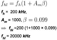
The correct answer is: 20000
Which of the following factors affect the frequency stability of an oscillator ?- a)temperature variation
- b)Inter element capacitances and stray capacitances
- c)output load
- d)coil size
Correct answer is option 'A,B,D'. Can you explain this answer?
Which of the following factors affect the frequency stability of an oscillator ?
a)
temperature variation
b)
Inter element capacitances and stray capacitances
c)
output load
d)
coil size
|
|
Jayant Mishra answered |
The stability of an oscillator depends on (i) inter element capacitances and stray capacitances (ii) temperature variation (iii) size of coil used It does not depend on the load.
The correct answers are: coil size, temperature variation, Inter element capacitances and stray capacitances
The correct answers are: coil size, temperature variation, Inter element capacitances and stray capacitances
Calculate the value of VCE (in Volts) for the circuit shown below. (β = 100 and VBE =0.7V).
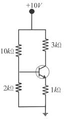
Correct answer is '6.22'. Can you explain this answer?
Calculate the value of VCE (in Volts) for the circuit shown below. (β = 100 and VBE =0.7V).


|
Pie Academy answered |
Let us use Thevenin’s theorem

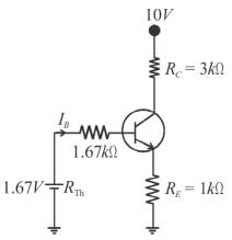
Now, applying KVL to Base circuit

= 9.45 μA
lC = 0.945mA
Now, Vcc = IcRc - VCE


The correct answer is: 6.22


Now, applying KVL to Base circuit

= 9.45 μA
lC = 0.945mA
Now, Vcc = IcRc - VCE


The correct answer is: 6.22
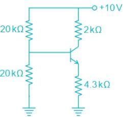
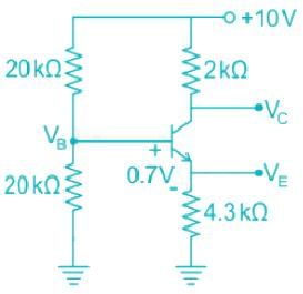
For the circuit shown below, the value of IC is:
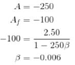
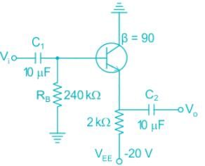 Correct answer is '4.12'. Can you explain this answer?
For the circuit shown below, the value of IC is:


|
|
Vivek Khatri answered |
Concept:
DC Analysis of BJT Amplifier
During the calculation of the DC parameter of a BJT amplifier, the capacitor is open-circuited.
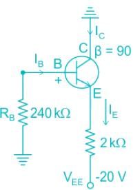
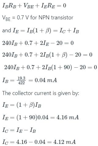
DC Analysis of BJT Amplifier
During the calculation of the DC parameter of a BJT amplifier, the capacitor is open-circuited.


For an amplifier, the base of an npn transistor must be.- a)negative with respect to emitter
- b)positive with respect to collector
- c)positive with respect to emitter
- d)OV
Correct answer is option 'C'. Can you explain this answer?
For an amplifier, the base of an npn transistor must be.
a)
negative with respect to emitter
b)
positive with respect to collector
c)
positive with respect to emitter
d)
OV
|
|
Jayant Mishra answered |
The base of an npn transistor must be positive with respect to emitter. The correct answer is: positive with respect to emitter
If for a silicon npn transistor, the base to emitter voltage (VBE) is 0.7Vand the collector to base voltage (VCB) is 0.2V, then the transistor is operating in the- a)inverse active mode
- b)cut-off mode
- c)saturation mode
- d)normal active mode
Correct answer is option 'D'. Can you explain this answer?
If for a silicon npn transistor, the base to emitter voltage (VBE) is 0.7Vand the collector to base voltage (VCB) is 0.2V, then the transistor is operating in the
a)
inverse active mode
b)
cut-off mode
c)
saturation mode
d)
normal active mode
|
|
Jayant Mishra answered |
VB = 0.7V (Forward-biased)
and VBC = -VCB
= -0.2V (Reverse-biased)
hence, the transistor operates in normal active mode.
The correct answer is: normal active mode
and VBC = -VCB
= -0.2V (Reverse-biased)
hence, the transistor operates in normal active mode.
The correct answer is: normal active mode
Figure shows a common emitter amplifier with β = 100. What is the maximum peak to peak input signal (in mV) for which distortion free output may be obtained Assume VBE = 0 rE = 20 Ω
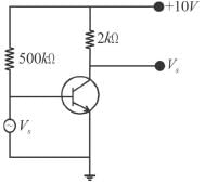
Correct answer is '80'. Can you explain this answer?
Figure shows a common emitter amplifier with β = 100. What is the maximum peak to peak input signal (in mV) for which distortion free output may be obtained Assume VBE = 0 rE = 20 Ω


|
|
Vedika Singh answered |
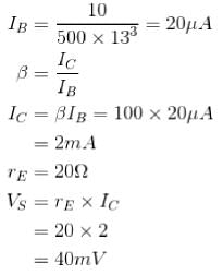
But for maximum peak to peak input signal

The correct answer is: 80
A bipolar junction transistor with one junction forward biased and either the collector or emitter open, operates in the.- a)active region
- b)saturation region
- c)cut-off region
- d)pinch-off region
Correct answer is option 'D'. Can you explain this answer?
A bipolar junction transistor with one junction forward biased and either the collector or emitter open, operates in the.
a)
active region
b)
saturation region
c)
cut-off region
d)
pinch-off region
|
|
Jayant Mishra answered |
When one junction is forward biased and either the collector or emitter is open, the BJT will operate in pinch-off region.
The correct answer is: pinch-off region
The correct answer is: pinch-off region
Which condition will saturate the BJT.- a)the emitter must be grounded
- b)

- c)Vcc must be atleast 10V
- d)

Correct answer is option 'D'. Can you explain this answer?
Which condition will saturate the BJT.
a)
the emitter must be grounded
b)

c)
Vcc must be atleast 10V
d)

|
|
Vedika Singh answered |
If  the BJT will go into the state of saturation.
The correct answer is:
 the BJT will go into the state of saturation.
The correct answer is:

With the positive probe on an NPN base, an ohmmeter reading between the other transistor terminals should be:- a)open
- b) infinite
- c)low resistance
- d)high resistance
Correct answer is option 'C'. Can you explain this answer?
With the positive probe on an NPN base, an ohmmeter reading between the other transistor terminals should be:
a)
open
b)
infinite
c)
low resistance
d)
high resistance
|
|
Arnav Sharma answered |
Explanation:
When an ohmmeter is connected to an NPN transistor with the positive probe on the base terminal, the reading between the other transistor terminals (collector and emitter) should be low resistance. This can be explained as follows:
1. NPN Transistor Structure:
An NPN transistor consists of three layers of semiconductor material: the emitter, base, and collector. These layers are doped with different types of impurities to create two pn junctions: the base-emitter junction (BE junction) and the base-collector junction (BC junction).
2. Base-Emitter Junction:
The base-emitter junction is forward-biased when a positive voltage is applied to the base terminal with respect to the emitter. This forward bias allows current to flow from the emitter to the base. The forward bias voltage causes the electrons from the emitter to move towards the base, creating a flow of majority charge carriers (electrons) through the base-emitter junction.
3. Base-Collector Junction:
The base-collector junction is reverse-biased when a positive voltage is applied to the collector terminal with respect to the base. This reverse bias prevents current flow through the base-collector junction. However, a small amount of current flows due to minority charge carriers (holes) from the base region being swept into the collector region.
4. Ohmmeter Reading:
When the positive probe of the ohmmeter is connected to the base terminal, it applies a positive voltage to the base with respect to the other transistor terminals.
- Collector-Emitter Reading: The collector-emitter junction is reverse-biased, so the ohmmeter reading between these terminals should be high resistance or open. This is because the reverse bias prevents current flow through the base-collector junction, and the ohmmeter measures the resistance between the collector and emitter.
- Base-Emitter Reading: The base-emitter junction is forward-biased, so the ohmmeter reading between these terminals should be low resistance. This is because the forward bias allows current flow through the base-emitter junction, and the ohmmeter measures the resistance between the base and emitter.
Therefore, when an ohmmeter is connected to an NPN transistor with the positive probe on the base terminal, the reading between the other transistor terminals should be low resistance. This indicates that the base-emitter junction is conducting, while the base-collector junction is not conducting.
What is the current gain for a common-base configuration where IE = 4.2 mA and IC = 4.0 mA?
Correct answer is between '0.95,0.96'. Can you explain this answer?
What is the current gain for a common-base configuration where IE = 4.2 mA and IC = 4.0 mA?
|
|
Vedika Singh answered |
Ie = 4.2ma (Given)
Ic = 4.0ma (Given)
The question follows the common base configuration in the circuit configuration of a bipolar transistor, where the emitter is the input electrode, collector is the output electrode and the base is reference electrode for both input and the output.
Thus,
Current gain = Ic / Ie =I(out)/I(in)
where, IC=Output Current and IE = Input Current
= 4 / 4.2
= 0.95
Therefore, the current gain for a common-base configuration is 0.95
Which of the following are associated with diffusion current.- a)base current
- b)emitter-base junction current
- c)emitter-base current
- d)base-collector junction current
Correct answer is option 'B,D'. Can you explain this answer?
Which of the following are associated with diffusion current.
a)
base current
b)
emitter-base junction current
c)
emitter-base current
d)
base-collector junction current
|
|
Jayant Mishra answered |
Emitter-base junction current and base-collector current are mainly due to diffusion current.
The correct answers are: emitter-base junction current, base-collector junction current
The correct answers are: emitter-base junction current, base-collector junction current
The equivalent electrical circuit of a vibrating crystal is as shown below.

- a)

- b)

- c)

- d)

Correct answer is option 'B'. Can you explain this answer?
The equivalent electrical circuit of a vibrating crystal is as shown below.


a)

b)

c)

d)

|
|
Jayant Mishra answered |
Since C and Cm are parallel, the equivalent capacitance is given as:
Ceq=c + cm
Now,

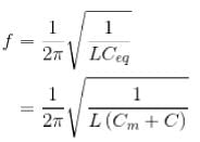
The correct answer is:
Ceq=c + cm
Now,


The correct answer is:

Calculate the minimum value of C2 (in μF) if the amplifier operate over a frequency range of 2kHz to 10kHz?
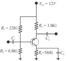
Correct answer is '1.42'. Can you explain this answer?
Calculate the minimum value of C2 (in μF) if the amplifier operate over a frequency range of 2kHz to 10kHz?


|
Pie Academy answered |
RE = 560Ω
XC of the bypass capacitor C2 should be

The capacitive value, at the minimum frequency of 2kHz

The correct answer is: 1.42
XC of the bypass capacitor C2 should be

The capacitive value, at the minimum frequency of 2kHz

The correct answer is: 1.42
The main function of coupling capacitor in an RC coupled common emitter amplifier is to :- a)increase the gain of the amplifier
- b)dc isolation
- c)increase the input impedance
- d)increase the output impedance
Correct answer is option 'B'. Can you explain this answer?
The main function of coupling capacitor in an RC coupled common emitter amplifier is to :
a)
increase the gain of the amplifier
b)
dc isolation
c)
increase the input impedance
d)
increase the output impedance
|
|
Jayant Mishra answered |
The cascaded amplifier, where an RC network is used for inter stage coupling is known as RC coupled amplifier. The main function of capacitor in RC coupling in common emitter amplifier is to isolate the dc .
The correct answer is: dc isolation
The correct answer is: dc isolation
Chapter doubts & questions for Bipolar Junction Transistors - Electronics for GATE 2025 is part of GATE Physics exam preparation. The chapters have been prepared according to the GATE Physics exam syllabus. The Chapter doubts & questions, notes, tests & MCQs are made for GATE Physics 2025 Exam. Find important definitions, questions, notes, meanings, examples, exercises, MCQs and online tests here.
Chapter doubts & questions of Bipolar Junction Transistors - Electronics for GATE in English & Hindi are available as part of GATE Physics exam.
Download more important topics, notes, lectures and mock test series for GATE Physics Exam by signing up for free.
Electronics for GATE
55 videos|28 docs|20 tests
|

Contact Support
Our team is online on weekdays between 10 AM - 7 PM
Typical reply within 3 hours
|
Free Exam Preparation
at your Fingertips!
Access Free Study Material - Test Series, Structured Courses, Free Videos & Study Notes and Prepare for Your Exam With Ease

 Join the 10M+ students on EduRev
|

|
Create your account for free
OR
Forgot Password
OR
Signup to see your scores
go up
within 7 days!
within 7 days!
Takes less than 10 seconds to signup

