Electronics and Communication Engineering (ECE) Exam > Electronics and Communication Engineering (ECE) Questions > In the circuit shown in the figure, the trans...
Start Learning for Free
In the circuit shown in the figure, the transistors M1 and M2 are operating in saturation. The channel length modulation coefficients of both the transistors are non-zero. The transconductance of the MOSFETs M 1 and M 2 are gm1 and gm2 , respectively, and the internal resistance of the MOSFETs M1 and M 2 are r01 and r02 , respectively.
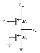
Ignoring the body effect, the ac small signal voltage gain ( ∂Vout /∂Vin) of the circuit is
- a)

- b)

- c)

- d)

Correct answer is option 'D'. Can you explain this answer?
| FREE This question is part of | Download PDF Attempt this Test |
Most Upvoted Answer
In the circuit shown in the figure, the transistors M1 and M2 are oper...
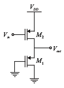
Given circuit is shown below,
Method 1 :
Channel length modulation coefficient λ≠ 0 , it means internal resistance of MOSFET M 1 and M 2 are not
zero.
The AC equivalent model of given circuit is shown below,
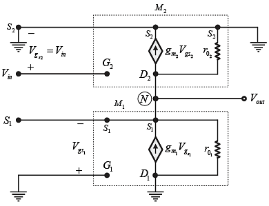
Applying KCL at node N,

So, put equation (ii) and (iii) into equation (i),
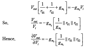
Hence, the correct option is (D).
Method 2 :
Given MOSFET arrangement is shown below,
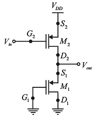
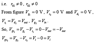
Channel length modulation coefficient λ≠ 0 , it means internal resistance of MOSFET M1 and M2 are not zero i.e., r01 ≠ 0 , r02 ≠ 0 .
AC equivalent circuit :
(i) All capacitors are short circuited.
(ii) All DC voltage sources replaced by ground.
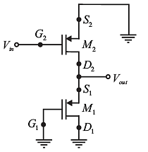
Here, drain ( D1) and gate (G1) of MOSFET (M1) are grounded, so it can be drawn as,
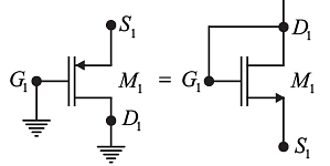
When drain and gate of MOSFET M1 are shorted to each other then it can be replaced by resistance of value  as shown below,
 as shown below,
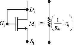
So, given circuit becomes as,
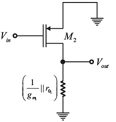
Above MOS circuit can redraw as,
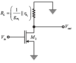
Here,  work as load for MOSFET (M2) , so small signal voltage gain of MOSFET (M2) is
 work as load for MOSFET (M2) , so small signal voltage gain of MOSFET (M2) is
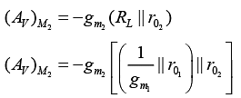
Hence, the correct option is (D).
Free Test
FREE
| Start Free Test |
Community Answer
In the circuit shown in the figure, the transistors M1 and M2 are oper...
Given circuit is shown below,

Method 1 :
Channel length modulation coefficient λ≠ 0 , it means internal resistance of MOSFET M 1 and M 2 are not
zero.

The AC equivalent model of given circuit is shown below,

Applying KCL at node N,

So, put equation (ii) and (iii) into equation (i),

Hence, the correct option is (D).
Method 2 :
Given MOSFET arrangement is shown below,

Channel length modulation coefficient λ≠ 0 , it means internal resistance of MOSFET M1 and M2 are not zero i.e., r01 ≠ 0 , r02 ≠ 0 .
AC equivalent circuit :
(i) All capacitors are short circuited.
(ii) All DC voltage sources replaced by ground.

Here, drain ( D1) and gate (G1) of MOSFET (M1) are grounded, so it can be drawn as,

When drain and gate of MOSFET M1 are shorted to each other then it can be replaced by resistance of value  as shown below,
 as shown below,
So, given circuit becomes as,

Above MOS circuit can redraw as,

Here,  work as load for MOSFET (M2) , so small signal voltage gain of MOSFET (M2) is
 work as load for MOSFET (M2) , so small signal voltage gain of MOSFET (M2) is
Hence, the correct option is (D).
Attention Electronics and Communication Engineering (ECE) Students!
To make sure you are not studying endlessly, EduRev has designed Electronics and Communication Engineering (ECE) study material, with Structured Courses, Videos, & Test Series. Plus get personalized analysis, doubt solving and improvement plans to achieve a great score in Electronics and Communication Engineering (ECE).

|
Explore Courses for Electronics and Communication Engineering (ECE) exam
|

|
Similar Electronics and Communication Engineering (ECE) Doubts
In the circuit shown in the figure, the transistors M1 and M2 are operating in saturation. The channel length modulation coefficients of both the transistors are non-zero. The transconductance of the MOSFETs M 1 and M 2 are gm1 and gm2 , respectively, and the internal resistance of the MOSFETs M1 and M 2 are r01 and r02 , respectively.Ignoring the body effect, the ac small signal voltage gain ( ∂Vout /∂Vin) of the circuit isa)b)c)d)Correct answer is option 'D'. Can you explain this answer?
Question Description
In the circuit shown in the figure, the transistors M1 and M2 are operating in saturation. The channel length modulation coefficients of both the transistors are non-zero. The transconductance of the MOSFETs M 1 and M 2 are gm1 and gm2 , respectively, and the internal resistance of the MOSFETs M1 and M 2 are r01 and r02 , respectively.Ignoring the body effect, the ac small signal voltage gain ( ∂Vout /∂Vin) of the circuit isa)b)c)d)Correct answer is option 'D'. Can you explain this answer? for Electronics and Communication Engineering (ECE) 2024 is part of Electronics and Communication Engineering (ECE) preparation. The Question and answers have been prepared according to the Electronics and Communication Engineering (ECE) exam syllabus. Information about In the circuit shown in the figure, the transistors M1 and M2 are operating in saturation. The channel length modulation coefficients of both the transistors are non-zero. The transconductance of the MOSFETs M 1 and M 2 are gm1 and gm2 , respectively, and the internal resistance of the MOSFETs M1 and M 2 are r01 and r02 , respectively.Ignoring the body effect, the ac small signal voltage gain ( ∂Vout /∂Vin) of the circuit isa)b)c)d)Correct answer is option 'D'. Can you explain this answer? covers all topics & solutions for Electronics and Communication Engineering (ECE) 2024 Exam. Find important definitions, questions, meanings, examples, exercises and tests below for In the circuit shown in the figure, the transistors M1 and M2 are operating in saturation. The channel length modulation coefficients of both the transistors are non-zero. The transconductance of the MOSFETs M 1 and M 2 are gm1 and gm2 , respectively, and the internal resistance of the MOSFETs M1 and M 2 are r01 and r02 , respectively.Ignoring the body effect, the ac small signal voltage gain ( ∂Vout /∂Vin) of the circuit isa)b)c)d)Correct answer is option 'D'. Can you explain this answer?.
In the circuit shown in the figure, the transistors M1 and M2 are operating in saturation. The channel length modulation coefficients of both the transistors are non-zero. The transconductance of the MOSFETs M 1 and M 2 are gm1 and gm2 , respectively, and the internal resistance of the MOSFETs M1 and M 2 are r01 and r02 , respectively.Ignoring the body effect, the ac small signal voltage gain ( ∂Vout /∂Vin) of the circuit isa)b)c)d)Correct answer is option 'D'. Can you explain this answer? for Electronics and Communication Engineering (ECE) 2024 is part of Electronics and Communication Engineering (ECE) preparation. The Question and answers have been prepared according to the Electronics and Communication Engineering (ECE) exam syllabus. Information about In the circuit shown in the figure, the transistors M1 and M2 are operating in saturation. The channel length modulation coefficients of both the transistors are non-zero. The transconductance of the MOSFETs M 1 and M 2 are gm1 and gm2 , respectively, and the internal resistance of the MOSFETs M1 and M 2 are r01 and r02 , respectively.Ignoring the body effect, the ac small signal voltage gain ( ∂Vout /∂Vin) of the circuit isa)b)c)d)Correct answer is option 'D'. Can you explain this answer? covers all topics & solutions for Electronics and Communication Engineering (ECE) 2024 Exam. Find important definitions, questions, meanings, examples, exercises and tests below for In the circuit shown in the figure, the transistors M1 and M2 are operating in saturation. The channel length modulation coefficients of both the transistors are non-zero. The transconductance of the MOSFETs M 1 and M 2 are gm1 and gm2 , respectively, and the internal resistance of the MOSFETs M1 and M 2 are r01 and r02 , respectively.Ignoring the body effect, the ac small signal voltage gain ( ∂Vout /∂Vin) of the circuit isa)b)c)d)Correct answer is option 'D'. Can you explain this answer?.
Solutions for In the circuit shown in the figure, the transistors M1 and M2 are operating in saturation. The channel length modulation coefficients of both the transistors are non-zero. The transconductance of the MOSFETs M 1 and M 2 are gm1 and gm2 , respectively, and the internal resistance of the MOSFETs M1 and M 2 are r01 and r02 , respectively.Ignoring the body effect, the ac small signal voltage gain ( ∂Vout /∂Vin) of the circuit isa)b)c)d)Correct answer is option 'D'. Can you explain this answer? in English & in Hindi are available as part of our courses for Electronics and Communication Engineering (ECE).
Download more important topics, notes, lectures and mock test series for Electronics and Communication Engineering (ECE) Exam by signing up for free.
Here you can find the meaning of In the circuit shown in the figure, the transistors M1 and M2 are operating in saturation. The channel length modulation coefficients of both the transistors are non-zero. The transconductance of the MOSFETs M 1 and M 2 are gm1 and gm2 , respectively, and the internal resistance of the MOSFETs M1 and M 2 are r01 and r02 , respectively.Ignoring the body effect, the ac small signal voltage gain ( ∂Vout /∂Vin) of the circuit isa)b)c)d)Correct answer is option 'D'. Can you explain this answer? defined & explained in the simplest way possible. Besides giving the explanation of
In the circuit shown in the figure, the transistors M1 and M2 are operating in saturation. The channel length modulation coefficients of both the transistors are non-zero. The transconductance of the MOSFETs M 1 and M 2 are gm1 and gm2 , respectively, and the internal resistance of the MOSFETs M1 and M 2 are r01 and r02 , respectively.Ignoring the body effect, the ac small signal voltage gain ( ∂Vout /∂Vin) of the circuit isa)b)c)d)Correct answer is option 'D'. Can you explain this answer?, a detailed solution for In the circuit shown in the figure, the transistors M1 and M2 are operating in saturation. The channel length modulation coefficients of both the transistors are non-zero. The transconductance of the MOSFETs M 1 and M 2 are gm1 and gm2 , respectively, and the internal resistance of the MOSFETs M1 and M 2 are r01 and r02 , respectively.Ignoring the body effect, the ac small signal voltage gain ( ∂Vout /∂Vin) of the circuit isa)b)c)d)Correct answer is option 'D'. Can you explain this answer? has been provided alongside types of In the circuit shown in the figure, the transistors M1 and M2 are operating in saturation. The channel length modulation coefficients of both the transistors are non-zero. The transconductance of the MOSFETs M 1 and M 2 are gm1 and gm2 , respectively, and the internal resistance of the MOSFETs M1 and M 2 are r01 and r02 , respectively.Ignoring the body effect, the ac small signal voltage gain ( ∂Vout /∂Vin) of the circuit isa)b)c)d)Correct answer is option 'D'. Can you explain this answer? theory, EduRev gives you an
ample number of questions to practice In the circuit shown in the figure, the transistors M1 and M2 are operating in saturation. The channel length modulation coefficients of both the transistors are non-zero. The transconductance of the MOSFETs M 1 and M 2 are gm1 and gm2 , respectively, and the internal resistance of the MOSFETs M1 and M 2 are r01 and r02 , respectively.Ignoring the body effect, the ac small signal voltage gain ( ∂Vout /∂Vin) of the circuit isa)b)c)d)Correct answer is option 'D'. Can you explain this answer? tests, examples and also practice Electronics and Communication Engineering (ECE) tests.

|
Explore Courses for Electronics and Communication Engineering (ECE) exam
|

|
Suggested Free Tests
Signup for Free!
Signup to see your scores go up within 7 days! Learn & Practice with 1000+ FREE Notes, Videos & Tests.


