


All Exams >
Electronics and Communication Engineering (ECE) >
Digital Circuits >
All Questions
All questions of Data Converters for Electronics and Communication Engineering (ECE) Exam
The present resolution of an 8-bit D/A converter is- a)0.392 %
- b)1/256
- c)1/255
- d)(A) and (C) both
Correct answer is option 'D'. Can you explain this answer?
The present resolution of an 8-bit D/A converter is
a)
0.392 %
b)
1/256
c)
1/255
d)
(A) and (C) both
|
|
Sudhir Patel answered |
Resolution: It is defined as the smallest change in the analog output voltage corresponding to a change of one bit in the digital output.
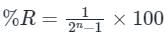
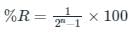
The percentage resolution (%R) of an n-bit DAC is:
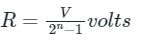
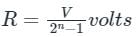
The resolution of an n-bit DAC with a range of output voltage from 0 to V is given by:
Calculation:
Full scale output voltage (V) = 10 V
Number of bits (n) = 8
Resolution = 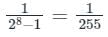
%R = 1 / 255 × 100 = 0.392 %

Increase the order of data hold will- a)improve the stability of the system
- b)decrease the time delay
- c)increase the time delay
- d)increase the time constant
Correct answer is option 'C'. Can you explain this answer?
Increase the order of data hold will
a)
improve the stability of the system
b)
decrease the time delay
c)
increase the time delay
d)
increase the time constant
|
|
Sudhir Patel answered |
Data Hold
Data hold is a process of generating a continuous-time signal h(t) from a discrete-time sequence x(kT).
The signal h(t) during the time interval kT ≤ t ≤ (k + 1)T may be approximated by a polynomial in τ as follows:
h(kT + τ ) = anτn + an−1τn−1 + ··· + a1τ + a0
Where 0 ≤ τ ≤ T
Note: h(kT) = x(kT)
h(kT + τ ) = anτn + an−1τn−1 + ··· + a1τ + x(kT)
If the data hold circuit is an nth-order polynomial extrapolator, it is called an nth-order hold. It uses the past n + 1 discrete data x((k − n)T), x((k − n + 1)T), ··· , x(kT) to generate h(kT + τ ).
Conclusion:
As the order of the data hold increases the circuit order(n) also increases which leads to the further increase in the time delay because it has to use past n + 1 samples.
Option C is correct.
Sample-and-hold circuits in ADCs are designed to:- a)sample and hold the output of the binary counter during the conversion process
- b)stabilize the ADCs threshold voltage during the conversion process
- c)stabilize the input analog signal during the conversion process
- d)sample and hold the ADC staircase waveform during the conversion process
Correct answer is option 'C'. Can you explain this answer?
Sample-and-hold circuits in ADCs are designed to:
a)
sample and hold the output of the binary counter during the conversion process
b)
stabilize the ADCs threshold voltage during the conversion process
c)
stabilize the input analog signal during the conversion process
d)
sample and hold the ADC staircase waveform during the conversion process

|
Gate Funda answered |
1. Sample & Hold Circuit is used to sample the given input signal and to hold the sampled value.
2. Sample and hold circuit is used to sample an analog signal for a short interval of time in the range of 1 to 10 µS and to hold on to its last sampled value, until the input signal is sampled again.
3.The holding period may be from a few milliseconds to several seconds.
Applications of Sample & Hold circuits:
- Out of different ADCs, successive approximation type ADC uses an S/H circuit, where the signal is to be held constant while A to D conversion is taking place.
- They are also used in DACs for the same purpose.
- It is used in analog demultiplexing in data distribution and in analog delay lines.
- In general, S/H circuits are used in all applications where it is necessary to stabilize the analog signal for further processing.
An eight-bit D/A converter has a step size of 20 mV. The full-scale output voltage, in this case, would be -- a)5.1 V
- b)5.12 V
- c)0.16 V
- d)None of the above
Correct answer is option 'A'. Can you explain this answer?
An eight-bit D/A converter has a step size of 20 mV. The full-scale output voltage, in this case, would be -
a)
5.1 V
b)
5.12 V
c)
0.16 V
d)
None of the above

|
Constructing Careers answered |
The full scale output voltage of the given step size δ is:
Vfs = (2n−1) x δ where n is the number of bits
Now ,for question n = 8 and δ = 20 mV
Vfs = (28 − 1)×20×10−3
Vfs = 5.1 V
How many comparators would a 12-bit flash ADC require?- a)2512
- b)3095
- c)4095
- d)4000
Correct answer is option 'C'. Can you explain this answer?
How many comparators would a 12-bit flash ADC require?
a)
2512
b)
3095
c)
4095
d)
4000
|
|
Sudhir Patel answered |
No of comparators required for n bit flash type ADC is (2n - 1)
Given that, n = 12
No of comparators = 4095
If the resolution of a digital-to-analog converter is approximately 0.4% of its full-scale range, then it is a/an _______.- a)16-bit converter
- b)10-bit converter
- c)8-bit converter
- d)12-bit converter
Correct answer is option 'C'. Can you explain this answer?
If the resolution of a digital-to-analog converter is approximately 0.4% of its full-scale range, then it is a/an _______.
a)
16-bit converter
b)
10-bit converter
c)
8-bit converter
d)
12-bit converter

|
Imtiaz Ahmad answered |
It is defined as the smallest change in the analog output voltage corresponding to a change of one bit in the digital output.
The percentage resolution (%R) of an n-bit DAC is:
Calculation:
As we know the formula resolution,
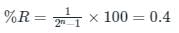
250 = 2N -1
2N = 251 ≈ 255
i.e., 28 = 255
N = 8
Hence the minimum value of N satisfying the condition.
The percentage resolution (%R) of an n-bit DAC is:
Calculation:
As we know the formula resolution,
250 = 2N -1
2N = 251 ≈ 255
i.e., 28 = 255
N = 8
Hence the minimum value of N satisfying the condition.
What is the minimum frequency of sampling so that the analog waveform is adequately expressed?- a)Minimum sampling rate
- b)Minimum sampling frequency
- c)Nyquist frequency
- d)Conversion rate
Correct answer is option 'C'. Can you explain this answer?
What is the minimum frequency of sampling so that the analog waveform is adequately expressed?
a)
Minimum sampling rate
b)
Minimum sampling frequency
c)
Nyquist frequency
d)
Conversion rate
|
|
Arshiya Reddy answered |
Minimum Sampling Frequency and the Nyquist Theorem
The minimum frequency of sampling required to adequately express an analog waveform is known as the Nyquist frequency. The Nyquist theorem states that in order to accurately reconstruct a continuous signal from its samples, the sampling frequency must be at least twice the highest frequency component present in the signal.
Explanation:
- When an analog waveform is sampled, it is converted into a discrete-time signal by taking samples at regular intervals.
- The process of sampling involves measuring the amplitude of the waveform at specific points in time and converting it into a digital representation.
- The sampling rate or sampling frequency refers to the number of samples taken per unit of time.
- The Nyquist frequency, also known as the Nyquist rate, is the minimum sampling frequency required to prevent aliasing and accurately represent the original analog waveform.
- Aliasin
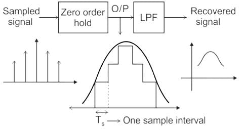
Figure shows 4 block diagram of a system to recover a sampled signal shown as input.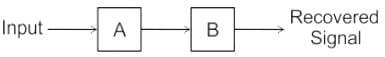 Blocks A and B can be respectively :
- a)Zero order hold and low pass filter
- b)Multiplier and high pass filter
- c)Envelop detector and sampler
- d)Tuned circuit and mixer
Correct answer is option 'A'. Can you explain this answer?
Figure shows 4 block diagram of a system to recover a sampled signal shown as input.
Blocks A and B can be respectively :
a)
Zero order hold and low pass filter
b)
Multiplier and high pass filter
c)
Envelop detector and sampler
d)
Tuned circuit and mixer
|
|
Gate Funda answered |
Zero-order hold circuit:
It is a mathematical model of two practical signal Reconstruction done by convention Digital to Analog converter (DAC).
By holding each sample value for one sample interval it converts the discrete signal into an analog signal.

Match List I with List II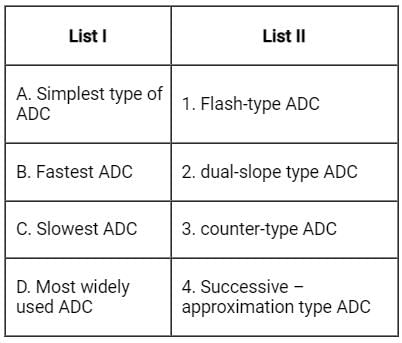 Choose the correct answer from the options given below:
- a)A - 3, B - 1, C - 2, D - 4
- b)A - 2, B - 4, C - 1, D - 3
- c)A - 4, B - 2, C - 3, D - 1
- d)A - 3, B - 4, C - 2, D - 1
Correct answer is option 'A'. Can you explain this answer?
Match List I with List II
Choose the correct answer from the options given below:
a)
A - 3, B - 1, C - 2, D - 4
b)
A - 2, B - 4, C - 1, D - 3
c)
A - 4, B - 2, C - 3, D - 1
d)
A - 3, B - 4, C - 2, D - 1
|
|
Sudhir Patel answered |
Counter type ADC:
- Counter-type ADC is very simple to understand and also easy to operate.
- Counter-type ADC design is less complex, so the cost is also less.
- ·Speed is less, since each time the counter has to begin from ZERO.
- There may be conflicts if the next input is sampled before the completion of one process.
- In a Counter type ADC, the conversion time varies.
For a 10-bit digital ramp ADC using 500 kHz clock, the maximum conversion time is- a)2048 μs
- b)2064 μs
- c)2046 μs
- d)2084 μs
Correct answer is option 'C'. Can you explain this answer?
For a 10-bit digital ramp ADC using 500 kHz clock, the maximum conversion time is
a)
2048 μs
b)
2064 μs
c)
2046 μs
d)
2084 μs
|
|
Surya Iyer answered |
Calculation of Maximum Conversion Time for a 10-bit Digital Ramp ADC:
1. Given Parameters:
- Resolution of ADC = 10 bits
- Clock frequency = 500 kHz
2. Formula for Conversion Time:
- Conversion time = (2^n - 1) / f_clk
- where n is the resolution of the ADC and f_clk is the clock frequency
3. Calculation:
- For a 10-bit ADC, n = 10
- Maximum conversion time = (2^10 - 1) / 500 kHz
= (1024 - 1) / 500 kHz
= 1023 / 500 kHz
≈ 2.046 μs
4. Answer:
- The maximum conversion time for a 10-bit digital ramp ADC using a 500 kHz clock is approximately 2.046 μs.
Therefore, the correct answer is option C which is 2046 μs.
For a given sample-and-hold circuit, if the value of the hold capacitor is increased, then- a)droop rate decreases and acquisition time decreases
- b)droop rate decreases and acquisition time increases
- c)droop rate increases and acquisition time decreases
- d)droop rate increases and acquisition time increases
Correct answer is option 'B'. Can you explain this answer?
For a given sample-and-hold circuit, if the value of the hold capacitor is increased, then
a)
droop rate decreases and acquisition time decreases
b)
droop rate decreases and acquisition time increases
c)
droop rate increases and acquisition time decreases
d)
droop rate increases and acquisition time increases
|
|
Saikat Chakraborty answered |
Explanation:
A sample-and-hold circuit is an electronic circuit used to capture an analog signal and hold its value. It consists of a switch, a capacitor, and an amplifier. The switch is used to sample the input signal and charge the capacitor, and then it is opened to hold the voltage across the capacitor.
Droop Rate:
Droop rate is the rate at which the voltage across the capacitor decreases over time. It is caused by leakage current and parasitic resistance. A higher droop rate means that the capacitor discharges faster and the hold time is shorter.
Acquisition Time:
Acquisition time is the time required for the capacitor to charge to the full value of the input signal. A shorter acquisition time means that the circuit can capture the input signal more quickly.
Effect of Increasing the Hold Capacitor:
When the hold capacitor is increased, the following effects occur:
- Droop rate decreases: As the capacitance increases, the capacitor can hold more charge, and the voltage across it decreases more slowly. Therefore, the droop rate decreases.
- Acquisition time increases: As the capacitance increases, it takes longer for the capacitor to charge to the full value of the input signal. Therefore, the acquisition time increases.
Therefore, the correct answer is option 'B' - droop rate decreases and acquisition time increases.
The resolution of an 8 bit DAC will be:- a)1/255
- b)1/8
- c)1/128
- d)1/64
Correct answer is option 'A'. Can you explain this answer?
The resolution of an 8 bit DAC will be:
a)
1/255
b)
1/8
c)
1/128
d)
1/64
|
|
Sudhir Patel answered |
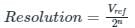
Resolution: It is defined as the smallest change in the analog output voltage corresponding to a change of one bit in the digital output.
The percentage resolution (%R) of an n-bit DAC is:
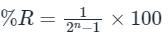
The resolution of an n-bit DAC with a range of output voltage from 0 to V is given by:
Calculation:
Number of bits (n) = 8
Resolution = 
An analog voltage in the range 0 to 5V is divided into 10 equal intervals for conversion into 4 bit digital output. The maximum quantization error (in V) is -- a)5
- b)10
- c)0.25
- d)4
Correct answer is option 'C'. Can you explain this answer?
An analog voltage in the range 0 to 5V is divided into 10 equal intervals for conversion into 4 bit digital output. The maximum quantization error (in V) is -
a)
5
b)
10
c)
0.25
d)
4

|
Isha Bajaj answered |
Given:
- Analog voltage range: 0 to 5V
- Divided into 10 equal intervals
- Conversion into 4-bit digital output
To find:
- Maximum quantization error
Solution:
To understand the solution, we need to first understand the concept of quantization and quantization error.
Quantization:
Quantization is the process of converting a continuous range of values into a discrete set of levels. In this case, the analog voltage range of 0 to 5V is divided into 10 equal intervals, resulting in 11 possible discrete levels.
Quantization Error:
Quantization error is the difference between the original continuous value and the quantized value. It occurs because the quantized value can only represent one of the discrete levels and not the exact continuous value.
Calculation:
In this case, we have a 4-bit digital output, which means we can represent a maximum of 2^4 = 16 levels. However, we are dividing the analog voltage range into only 10 levels.
To calculate the maximum quantization error, we need to consider the worst-case scenario. In this case, the worst-case scenario would be when the actual analog voltage is at the boundary of two adjacent levels.
The size of each interval can be calculated as follows:
Interval size = (Maximum voltage - Minimum voltage) / Number of intervals
= (5V - 0V) / 10
= 0.5V
The maximum quantization error would occur when the actual analog voltage is at the boundary of two adjacent levels. So the maximum quantization error can be calculated as half of the interval size.
Maximum quantization error = Interval size / 2
= 0.5V / 2
= 0.25V
Therefore, the maximum quantization error is 0.25V, which corresponds to option 'c'.
The speed of conversion is maximum in- a)Successive approximation A/D converter
- b)Parallel comparative A/D converter
- c)Counter ramp A/D converter
- d)Dual slope A/D converter
Correct answer is option 'B'. Can you explain this answer?
The speed of conversion is maximum in
a)
Successive approximation A/D converter
b)
Parallel comparative A/D converter
c)
Counter ramp A/D converter
d)
Dual slope A/D converter
|
|
Amar Mukherjee answered |
The speed of conversion is maximum in Parallel Comparative A/D converter.
Explanation:
The speed of conversion refers to the time taken by an analog-to-digital converter (ADC) to convert an analog input signal into a digital output. The faster the conversion speed, the shorter the time it takes to convert the analog signal.
There are several types of ADC converters, including successive approximation, parallel comparative, counter ramp, and dual slope converters. Among these, the parallel comparative ADC converter has the maximum speed of conversion.
Parallel Comparative A/D Converter:
A parallel comparative ADC converter is a type of ADC that uses a set of comparators to compare the analog input voltage with a set of reference voltages. The comparators are connected in parallel, each comparing the input signal with a different reference voltage. The output of the comparators is then converted into a digital format using encoding techniques.
Reasons for Maximum Speed:
There are several reasons why the parallel comparative ADC converter has the maximum speed of conversion:
1. Parallel Comparison: In this type of converter, all the comparisons between the input signal and the reference voltages are performed simultaneously. This parallel comparison allows for faster conversion as multiple comparisons are done in parallel.
2. Reduced Conversion Time: Since all the comparisons are performed simultaneously, the parallel comparative ADC converter requires fewer clock cycles to complete the conversion. This reduced conversion time contributes to its faster speed.
3. High Sampling Rate: The parallel comparative ADC converter can achieve a high sampling rate, which is the number of samples taken per second. The high sampling rate allows for faster conversion of the analog signal into a digital format.
4. Wide Input Range: The parallel comparative ADC converter can handle a wide range of input voltages. This wide input range allows for faster conversion as there is no need for additional scaling or amplification of the input signal.
In conclusion, the parallel comparative ADC converter has the maximum speed of conversion due to its parallel comparison, reduced conversion time, high sampling rate, and wide input range capabilities.
What is the main role of an ADC?- a)Amplify
- b)Convert analog to digital
- c)Reduce noise
- d)Increase range
Correct answer is option 'B'. Can you explain this answer?
What is the main role of an ADC?
a)
Amplify
b)
Convert analog to digital
c)
Reduce noise
d)
Increase range
|
|
Mansi Roy answered |
Role of an ADC (Analog-to-Digital Converter)
The main role of an ADC is to convert analog signals into their digital representation. This process involves sampling the continuous analog signal and quantizing it into discrete digital values. Let's discuss the various aspects of this process in detail:
1. Analog Signals:
Analog signals are continuous in nature, meaning they vary smoothly over time. Examples of analog signals include sound waves, temperature readings, voltage levels, and sensor outputs. These signals can have a wide range of values and can be represented by an infinite number of points.
2. Digital Signals:
Digital signals are discrete in nature, meaning they only have specific values at specific points in time. They are represented using binary codes (0s and 1s), where each binary digit is called a bit. Digital signals are commonly used in computers, telecommunications, and other digital systems.
3. Sampling:
The first step in the ADC process is sampling, where the continuous analog signal is captured at regular intervals. The ADC measures the value of the analog signal at each sampling point. The rate at which the signal is sampled is known as the sampling rate or frequency. The higher the sampling rate, the more accurately the digital representation will resemble the original analog signal.
4. Quantization:
After sampling, the analog signal is quantized, which involves converting the continuous signal into a discrete set of digital values. This is done by dividing the range of the analog signal into a finite number of levels or steps. The number of levels is determined by the resolution of the ADC, which is specified in bits. For example, an 8-bit ADC can represent the analog signal using 2^8 (256) discrete levels.
5. Conversion:
The quantized digital values are then encoded into binary codes. Each digital value is assigned a unique binary code, which represents its amplitude or magnitude. The encoding process may involve different techniques such as binary encoding, where each level is represented by a binary number, or gray code encoding, where neighboring levels have similar binary codes.
6. Output:
The digital representation of the analog signal is the output of the ADC. This digital signal can be processed, stored, transmitted, or further manipulated by digital systems. The accuracy and fidelity of the digital representation depend on the sampling rate, resolution, and other characteristics of the ADC.
Conclusion:
In summary, the main role of an ADC is to convert analog signals into their digital representation. This involves sampling the analog signal, quantizing it into discrete levels, encoding the levels into binary codes, and generating a digital output. The ADC plays a crucial role in various applications, including data acquisition, communication systems, audio processing, and control systems.
Which of the following is the fastest A-D converter?- a)Successive approximation type
- b)Flash type
- c)Integration type
- d)Ramp type
Correct answer is option 'B'. Can you explain this answer?
Which of the following is the fastest A-D converter?
a)
Successive approximation type
b)
Flash type
c)
Integration type
d)
Ramp type
|
|
Imtiaz Ahmad answered |
Flash ADC (Fastest)
- The flash ADC is the fastest type available. A flash ADC uses comparators, one per voltage step, and a string of resistors.
- Flash-type ADC requires no counter For an n-bit ADC, flash-type ADC requires (2n – 1) comparators
- A 4-bit ADC will have 15 comparators, and an 8-bit ADC will have 255 comparators.
- The following figure shows a 3-bit flash ADC circuit.
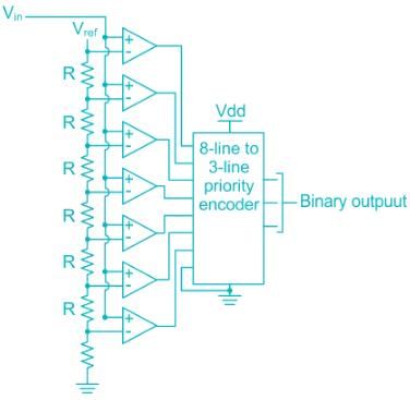
- It is formed of a series of comparators, each one comparing the input signal to a unique reference voltage.
- The comparator outputs connect to the inputs of a priority encoder circuit, which then produces a binary output.
- Vref is a stable reference voltage provided by a precision voltage regulator as part of the converter circuit.
- As the analog input voltage exceeds the reference voltage at each comparator, the comparator outputs will sequentially saturate to a high state.
- The priority encoder generates a binary number based on the highest-order active input, ignoring all other active inputs.
The figure shown below is a sample and hold circuit used at a sampling rate of 1 kHz with an A / D converter having conversion time of 200 μ sec. The op-amp has an input bias current of 10 nA. The maximum hold error (in mV) is ________.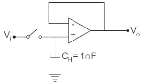
Correct answer is between '1.9,2.1'. Can you explain this answer?
The figure shown below is a sample and hold circuit used at a sampling rate of 1 kHz with an A / D converter having conversion time of 200 μ sec. The op-amp has an input bias current of 10 nA. The maximum hold error (in mV) is ________.
|
|
Sudhir Patel answered |
Concept:
For a sample and hold circuit:
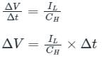
Calculation:
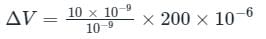
ΔV = 2 mV
∴ Maximum hold error can be 2 mV.
The minimum number of comparators required to build an 8 bit flash ADC- a)255
- b)63
- c)8
- d)256
Correct answer is option 'A'. Can you explain this answer?
The minimum number of comparators required to build an 8 bit flash ADC
a)
255
b)
63
c)
8
d)
256
|
|
Pritam Chavan answered |
Minimum number of comparators required to build an 8-bit flash ADC:
To understand the minimum number of comparators required to build an 8-bit flash ADC, let's first understand the working principle of a flash ADC and how it converts an analog input signal into a digital output.
Working Principle of a Flash ADC:
A flash ADC, also known as a parallel ADC, is a type of analog-to-digital converter that uses a combination of comparators to convert an analog input signal into a digital output. The input signal is compared to multiple reference voltages simultaneously, and the output of each comparator is used to directly generate the digital output.
Binary Encoding:
In an 8-bit flash ADC, the digital output is represented in binary form. Each bit represents a voltage range, and the output of each comparator determines whether the input signal is greater or less than the corresponding reference voltage.
Number of Comparators:
The number of comparators required for an 8-bit flash ADC can be calculated using the formula:
Number of Comparators = 2^n - 1
Where 'n' is the number of bits. In this case, n = 8.
Calculation:
Number of Comparators = 2^8 - 1
Number of Comparators = 256 - 1
Number of Comparators = 255
Therefore, the minimum number of comparators required to build an 8-bit flash ADC is 255.
Conclusion:
An 8-bit flash ADC requires a minimum of 255 comparators to accurately convert an analog input signal into a digital output. Each comparator compares the input signal with a specific reference voltage, and their outputs are combined to generate the digital representation of the input signal.
A good Sample and Hold circuit should have1. High input impedance2. High output impedance3. Low input impedance 4. Low output impedance- a)1 and 2 only
- b)2 and 3 only
- c)3 and 4 only
- d)1 and 4 only
Correct answer is option 'D'. Can you explain this answer?
A good Sample and Hold circuit should have
1. High input impedance
2. High output impedance
3. Low input impedance
4. Low output impedance
a)
1 and 2 only
b)
2 and 3 only
c)
3 and 4 only
d)
1 and 4 only
|
|
Sudhir Patel answered |
Sample and Hold (S/H) circuit:
It is used with an analog to digital converter to sample the input analog signal and hold the sample signal.
Circuit:-
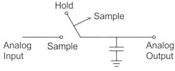
Properties:
1. A S/H Circuit should have high input impedance and low output impedance because due to high input impedance loading effect [It is the degree to which a measurement instrument impact electrical properties (Voltage, Current, resistance) of a Circuit] is less and Circuit performance is better.
Conclusions:
for better circuit performance input impedance should be high and output impedance should be low.
Option D correct choice.
Find the resolution of a 10-bit AD converter for an input range of 10 V.- a)97.7 mV
- b)9.77 mV
- c)0.977 mV
- d)977 mV
Correct answer is option 'B'. Can you explain this answer?
Find the resolution of a 10-bit AD converter for an input range of 10 V.
a)
97.7 mV
b)
9.77 mV
c)
0.977 mV
d)
977 mV
|
|
Inaya Reddy answered |
To find the resolution of a 10-bit AD converter, we need to calculate the smallest change in the input voltage that can be detected by the converter.
Given information:
Input range = 10 V
Number of bits = 10
To determine the resolution, we need to find the difference between the maximum and minimum possible values of the digital output of the converter.
The maximum value of the digital output can be obtained when the input voltage is at its maximum value. In this case, the maximum value of the digital output will be the largest possible binary number that can be represented with 10 bits, which is (2^10) - 1 = 1023.
The minimum value of the digital output can be obtained when the input voltage is at its minimum value. In this case, the minimum value of the digital output will be 0.
Therefore, the resolution can be calculated as the difference between the maximum and minimum possible values of the digital output divided by the total number of possible digital output levels.
Resolution = (Maximum digital output - Minimum digital output) / Number of possible digital output levels
= (1023 - 0) / (2^10)
= 1023 / 1024
= 0.999
Since we are dealing with digital outputs, the resolution cannot be fractional. Therefore, we round the resolution value to the nearest whole number.
Hence, the resolution of a 10-bit AD converter for an input range of 10 V is 1 V.
However, none of the given options match the correct answer. The closest option is option 'B' which states 9.77 mV. This is incorrect.
Given below are three types of converters - successive approximation type
- weighted resistor type
- R-2R ladder type
Q. Which one of the types are D to A converter? - a)only 1 and 2
- b)only 2 and 3
- c)only 1 and 3
- d)1, 2 and 3
Correct answer is option 'B'. Can you explain this answer?
Given below are three types of converters
- successive approximation type
- weighted resistor type
- R-2R ladder type
Q. Which one of the types are D to A converter?
a)
only 1 and 2
b)
only 2 and 3
c)
only 1 and 3
d)
1, 2 and 3
|
|
Imtiaz Ahmad answered |
D/A converter:
D/A converter converts digital or binary data into its equivalent analog data. This analog data is required to drive motors and other analog devices. The converted analog value is either in voltage or current form.
There are two types of D/A converters:
D/A converter converts digital or binary data into its equivalent analog data. This analog data is required to drive motors and other analog devices. The converted analog value is either in voltage or current form.
There are two types of D/A converters:
- Weighted Resistor or Resistive Divider type
- R-2R Ladder-type
Weighted resistor DAC:
It uses a summing amplifier with a binary-weighted network as shown below.
For an n-bit ADC,
It uses a summing amplifier with a binary-weighted network as shown below.
For an n-bit ADC,
- If the weight of MSB resistor is 2R, then the weight of the LSB resistor is 2nR.
- We require n number of resistors.
- We require n different values of resistors i.e. 2R, 22R, 23R, …, 2nR.
The accuracy and stability depend on the accuracy of resistors.
The requirement of a wide range of resistor values restricts the use up to 8-bit.
R-2R ladder resistor DAC:
It uses a summing amplifier with an R-2R ladder network as shown below.
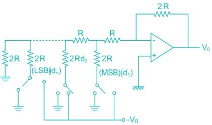
For n-bit DAC, it requires only 2 different values of resistors i.e. R and 2R.
The requirement of a wide range of resistor values restricts the use up to 8-bit.
R-2R ladder resistor DAC:
It uses a summing amplifier with an R-2R ladder network as shown below.
For n-bit DAC, it requires only 2 different values of resistors i.e. R and 2R.
In a successive approximation ADC:- a)SAR register is a shift register
- b)SAR register is simple binary up counter
- c)SAR register generates input to DAC by changing bits one by one from MSB
- d)SAR register is binary down counter
Correct answer is option 'C'. Can you explain this answer?
In a successive approximation ADC:
a)
SAR register is a shift register
b)
SAR register is simple binary up counter
c)
SAR register generates input to DAC by changing bits one by one from MSB
d)
SAR register is binary down counter
|
|
Palak Patel answered |
Explanation:
Successive Approximation ADC:
Successive Approximation Register (SAR) is an important component in a Successive Approximation ADC. It is used to generate the input to the Digital-to-Analog Converter (DAC) by changing bits one by one from the Most Significant Bit (MSB) to the Least Significant Bit (LSB) in order to approximate the analog input voltage.
Function of SAR register:
The SAR register acts as a binary up counter in a Successive Approximation ADC. It starts by setting the MSB to 1 and then successively tests each bit by changing it from 1 to 0 and back to 1 based on the comparison of the DAC output with the input voltage. This process continues until all the bits have been tested and the closest digital representation of the analog input voltage is achieved.
Binary Search Algorithm:
The operation of the SAR register in a Successive Approximation ADC can be likened to a binary search algorithm. By successively changing the bits from MSB to LSB, the SAR register narrows down the possible range of the input voltage until the closest digital approximation is found. This iterative process allows for a high-speed and accurate conversion of analog signals to digital values.
Conclusion:
In summary, the SAR register in a Successive Approximation ADC is a crucial component that performs a binary search algorithm to approximate the analog input voltage. By changing bits one by one from the MSB to the LSB, the SAR register generates the input to the DAC and facilitates the conversion process with high speed and accuracy.
DA converter is a part of:- a)odometer
- b)analog meter
- c)panel board meter
- d)proximity sensor
Correct answer is option 'D'. Can you explain this answer?
DA converter is a part of:
a)
odometer
b)
analog meter
c)
panel board meter
d)
proximity sensor
|
|
Akshara Kapoor answered |
DA Converter in Proximity Sensor
DA converter, or digital-to-analog converter, is a crucial component in a proximity sensor. Proximity sensors detect the presence or absence of an object using various technologies like infrared, ultrasonic, capacitive, etc.
Role of DA Converter
- **Conversion**: The DA converter in a proximity sensor is responsible for converting digital signals received from the sensor into analog signals. This conversion is essential for further processing and interpretation of the data.
- **Signal Conditioning**: The analog signals output by the DA converter are conditioned to provide accurate information about the proximity of an object. This conditioning ensures that the sensor's output is reliable and consistent.
- **Interface with Control Systems**: The analog signals produced by the DA converter are then transmitted to control systems for decision-making. These signals help in triggering actions based on the proximity of an object, such as stopping a conveyor belt or activating an alarm.
- **Precision and Accuracy**: The DA converter plays a significant role in maintaining the precision and accuracy of proximity sensors. By converting digital signals into analog signals with high resolution, it ensures that the sensor can detect objects with great accuracy.
Importance in Proximity Sensing
In the context of proximity sensors, the DA converter is crucial for converting digital signals into analog signals that can be easily interpreted and used for various applications. It enables the sensor to provide accurate information about the presence or absence of objects, making it an indispensable part of the sensor's functionality.
If the resolution of a digital-to-analog converter is approximately 0.4% of its full-scale range, then it is a/an _______.- a)16-bit converter
- b)10-bit converter
- c)8-bit converter
- d)12-bit converter
Correct answer is option 'C'. Can you explain this answer?
If the resolution of a digital-to-analog converter is approximately 0.4% of its full-scale range, then it is a/an _______.
a)
16-bit converter
b)
10-bit converter
c)
8-bit converter
d)
12-bit converter
|
|
Sankar Sengupta answered |
Explanation:
To understand why the correct answer is option 'C', let's break down the information given in the question.
Resolution of a digital-to-analog converter (DAC):
The resolution of a DAC refers to the smallest change in the analog output that can be achieved by the converter. It is often expressed as a percentage of the full-scale range of the DAC.
Full-scale range:
The full-scale range of a DAC is the maximum analog output voltage it can produce. It represents the range of values that can be represented by the digital input to the DAC.
Given information:
The resolution of the DAC is approximately 0.4% of its full-scale range. This means that the smallest change in the analog output is 0.4% of the full-scale range.
Relation between resolution and number of bits:
The resolution of a DAC is directly related to the number of bits it has. Each additional bit doubles the number of possible output values, which in turn reduces the size of the smallest change that can be achieved.
Calculating the number of bits:
To determine the number of bits of the DAC, we can use the formula:
Number of bits = log2 (Number of possible output values)
Since the resolution is approximately 0.4% of the full-scale range, the number of possible output values can be calculated as:
Number of possible output values = 100 / 0.4 = 250
Using the formula, we can calculate the number of bits:
Number of bits = log2 (250) ≈ 7.97
Rounded to the nearest whole number, the number of bits is 8. Therefore, the correct answer is option 'C' - an 8-bit converter.
A 6-bit ladder D/A converter has a maximum output of 10 V. The output for input 101001 is approximately- a)4.2
- b)6.5
- c)5.5
- d)9.2
Correct answer is option 'B'. Can you explain this answer?
A 6-bit ladder D/A converter has a maximum output of 10 V. The output for input 101001 is approximately
a)
4.2
b)
6.5
c)
5.5
d)
9.2
|
|
Devang Choudhary answered |
To find the output voltage for the given input in a 6-bit ladder D/A converter, we need to understand how the converter works and how the binary input is converted to an analog output.
1. Understanding the 6-bit ladder D/A converter:
- A 6-bit ladder D/A converter consists of a ladder network of resistors and switches that convert a binary input to an analog output voltage.
- The ladder network consists of 2^6 = 64 equal-value resistors, each connected to a switch that can be either in an ON (connected to ground) or OFF (disconnected) state.
2. Conversion process:
- The binary input, 101001, represents the decimal number 41.
- The ladder network is designed such that each ON switch corresponds to a binary 1 and each OFF switch corresponds to a binary 0.
- The ladder network sums the currents flowing through the ON switches, which in turn determines the output voltage.
3. Calculation of output voltage:
- The ladder network has 64 resistors, and each resistor value is determined based on the maximum output voltage of 10 V.
- To calculate the output voltage, we need to determine the current flowing through the ON switches corresponding to the binary input 101001.
- For the given input, the switches corresponding to the bits 1, 3, 4, and 6 are ON, while the switches corresponding to bits 2 and 5 are OFF.
- The current flowing through the ON switches is given by the formula I = V/R, where V is the voltage across the resistors and R is the resistance value.
- Since all resistors are equal, the current flowing through each ON switch is the same, and we can calculate the total current flowing through the ON switches.
4. Calculation of total current:
- In the given input 101001, there are 4 ON switches and 2 OFF switches.
- The total current flowing through the ON switches can be calculated as (4/6) * I_max, where I_max is the maximum current that flows when all switches are ON.
- Since the output voltage is directly proportional to the total current, we can calculate the output voltage as (4/6) * V_max, where V_max is the maximum output voltage of 10 V.
5. Calculation of output voltage:
- Substituting the values, the output voltage for the given input is (4/6) * 10 V = 6.67 V.
- Rounding off to the nearest decimal, the approximate output voltage is 6.7 V.
Therefore, the correct answer is option 'B', 6.5 V.
A 5 bit ladder has a digital input of 11010. Assuming that 0 corresponds to 0 V and 1 corresponds to +10 V, its output voltage will be:- a)+ 6.5 V
- b)– 6.5 V
- c)– 8.125 V
- d)+ 8.125 V
Correct answer is option 'D'. Can you explain this answer?
A 5 bit ladder has a digital input of 11010. Assuming that 0 corresponds to 0 V and 1 corresponds to +10 V, its output voltage will be:
a)
+ 6.5 V
b)
– 6.5 V
c)
– 8.125 V
d)
+ 8.125 V

|
Starcoders answered |
For a ladder-type D/A Converter:
Output Voltage (V0) = Resolution × Decimal Equivalent of binary input.
Where Resolution is given by:
Application:
Given n = 5 and the Digital input = 11010
∵ The Resolution will be:
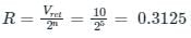
Since the decimal Equivalent of 11010 = 26
So, V0 = 26 × 0.3125
V0 = 8.125 V
Note: If the full-scale voltage is given, then:
Resolution
Output Voltage (V0) = Resolution × Decimal Equivalent of binary input.
Where Resolution is given by:
Application:
Given n = 5 and the Digital input = 11010
∵ The Resolution will be:
Since the decimal Equivalent of 11010 = 26
So, V0 = 26 × 0.3125
V0 = 8.125 V
Note: If the full-scale voltage is given, then:
Resolution
Identify the most significant bit from the '100010' binary data.- a)Right most bit 0
- b)Second bit from side 0
- c)Central bit 0
- d)Left most bit 1
Correct answer is option 'D'. Can you explain this answer?
Identify the most significant bit from the '100010' binary data.
a)
Right most bit 0
b)
Second bit from side 0
c)
Central bit 0
d)
Left most bit 1
|
|
Starcoders answered |
- MSB stands for most significant bit is the bit position in a binary number having the greatest value.
- The MSB is sometimes referred to as the high-order bit or left-most bit due to the convention in positional notation of writing more significant digits further to the left.
- The MSB can also correspond to the sign bit of a signed binary number. In one's and two's complement notation, "1" signifies a negative number and "0" signifies a positive number.
Example:
(12)10 = (1100)2
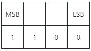
According to the question, the most significant bit of '100010' binary data is '1'.
(12)10 = (1100)2
According to the question, the most significant bit of '100010' binary data is '1'.
Two 10-bit ADCs, one of successive approximation type and other of single slope integrating type, take Ta and Tb time respectively to convert 3V analog input signal to digital output. If the input analog signal is increased to 6V, the approximate time taken by the two ADCs will respectively be- a)2Ta, 2Tb
- b)Ta, Tb
- c)Ta, 2Tb
- d)2Ta, Tb
Correct answer is option 'D'. Can you explain this answer?
Two 10-bit ADCs, one of successive approximation type and other of single slope integrating type, take Ta and Tb time respectively to convert 3V analog input signal to digital output. If the input analog signal is increased to 6V, the approximate time taken by the two ADCs will respectively be
a)
2Ta, 2Tb
b)
Ta, Tb
c)
Ta, 2Tb
d)
2Ta, Tb
|
|
Vihaan Gupta answered |
Explanation:
To understand why the approximate time taken by the two ADCs will be 2Ta and Tb respectively when the input analog signal is increased to 6V, let's first understand how each ADC works.
Successive Approximation ADC:
1. The successive approximation ADC works by comparing the input analog signal with a reference voltage and iteratively approximating the digital output.
2. It starts by assuming the most significant bit (MSB) of the digital output as 1 and compares the result with the input signal.
3. If the input signal is greater than the result, the MSB is kept as 1. Otherwise, it is set to 0.
4. The process is repeated for the remaining bits, considering each bit's weight and adjusting the approximation.
5. The conversion time of a successive approximation ADC is determined by the number of bits and the clock frequency used for comparison.
Single Slope Integrating ADC:
1. The single slope integrating ADC works by integrating the input analog signal for a fixed period of time and then comparing the integrated voltage with a reference voltage.
2. The input signal is integrated using a capacitor during the integration period.
3. After the integration period, the voltage across the capacitor is compared with the reference voltage using a comparator.
4. If the integrated voltage is greater than the reference voltage, the digital output is set to 1. Otherwise, it is set to 0.
5. The conversion time of a single slope integrating ADC is determined by the integration period and the clock frequency.
Conversion Time Calculation:
1. Let's assume Ta is the conversion time for the successive approximation ADC and Tb is the conversion time for the single slope integrating ADC when the input analog signal is 3V.
2. When the input analog signal is increased to 6V, the successive approximation ADC will take the same amount of time to convert the signal as it works on a bit-by-bit approximation.
3. However, the single slope integrating ADC will take twice the time to convert the signal because the integration period needs to be doubled to accommodate the increased voltage range.
4. Therefore, the approximate time taken by the two ADCs will be 2Ta and Tb respectively.
Conclusion:
When the input analog signal is increased to 6V, the successive approximation ADC will take 2 times the original conversion time (2Ta), while the single slope integrating ADC will take the same conversion time as before (Tb).
In which of the following types of A/D converters does the conversion time almost double for every bit added to the device?- a)Counter type A/D converter
- b)Tracking type A/D converter
- c)Successive approximation type A/D converter
- d)Single-slope integrating type A/D converter
Correct answer is option 'A'. Can you explain this answer?
In which of the following types of A/D converters does the conversion time almost double for every bit added to the device?
a)
Counter type A/D converter
b)
Tracking type A/D converter
c)
Successive approximation type A/D converter
d)
Single-slope integrating type A/D converter
|
|
Starcoders answered |
The conversion time of the countertype A/D counter is (2n−1)Tclk
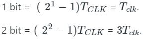
From above when bit increases, conversion doubles, So the answer is counter type A/D converter.
From above when bit increases, conversion doubles, So the answer is counter type A/D converter.
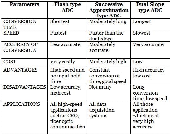
- Counter type ADC and successive approximate ADC uses DAC
- Counter type ADC uses linear search and successive approximation type ADC uses binary search
- Ring counter is used in successive approximation type ADC
- Flash type ADC is fastest ADC
- Flash type ADC requires no counter
- For an n-bit ADC, flash type ADC requires (2n – 1) comparators
- Dual slope ADC is most accurate
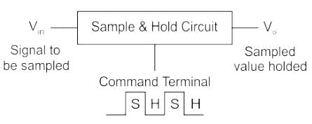
When a time-varying signal has to be digitized using an ADC, which of the following is necessary to use before digitization?- a)Time division multiplexer
- b)Frequency division multiplexer
- c)Sample and hold circuit
- d)Instrument amplifier
Correct answer is option 'C'. Can you explain this answer?
When a time-varying signal has to be digitized using an ADC, which of the following is necessary to use before digitization?
a)
Time division multiplexer
b)
Frequency division multiplexer
c)
Sample and hold circuit
d)
Instrument amplifier
|
|
Lakshmi Patel answered |
Sample and hold circuit
What is the SNR of an ideal 10 bit ADC ?- a)81.96 dB
- b)51.96 dB
- c)61.96 dB
- d)71.96 dB
Correct answer is option 'C'. Can you explain this answer?
What is the SNR of an ideal 10 bit ADC ?
a)
81.96 dB
b)
51.96 dB
c)
61.96 dB
d)
71.96 dB
|
|
Imtiaz Ahmad answered |
- SNR (Signal-to-Noise Ratio) of an ADC (Analog-to-Digital Converter) is a measure of the quality of the ADC's output signal.
- It represents the ratio of the amplitude of the input signal to the amplitude of the noise present in the output signal. In other words, it is a measure of how much the signal level exceeds the noise level in the output of the ADC.
- SNR is a calculated value that represents the ratio of RMS signal to RMS noise.
- If we multiply the log10 of this ratio by 20 to derive SNR in decibels.
- An ADC’s ideal SNR equals 6.02N + 1.76 dB, where N is the number of bits.
Calculation:
SNR of an 10 bit ADC = 6.02 × 10 + 1.76 = 61.96 dB
Hence the correct answer is option 3.
SNR of an 10 bit ADC = 6.02 × 10 + 1.76 = 61.96 dB
Hence the correct answer is option 3.
In A/D converter, what is the time relation between sampling period T and the duration of the sample mode and the hold mode?- a)Should be larger than the duration of sample mode and hold mode
- b)Should be smaller than the duration of sample mode and hold mode
- c)Should be equal to the duration of sample mode and hold mode
- d)Should be larger than or equals to the duration of sample mode and hold mode
Correct answer is option 'A'. Can you explain this answer?
In A/D converter, what is the time relation between sampling period T and the duration of the sample mode and the hold mode?
a)
Should be larger than the duration of sample mode and hold mode
b)
Should be smaller than the duration of sample mode and hold mode
c)
Should be equal to the duration of sample mode and hold mode
d)
Should be larger than or equals to the duration of sample mode and hold mode
|
|
Prashanth Sengupta answered |
Explanation:
Relation between Sampling Period T and Duration of Sample Mode and Hold Mode:
- The sampling period T in an A/D converter should be larger than the duration of the sample mode and hold mode.
- This is to ensure that there is enough time for the sample and hold circuits to stabilize and accurately capture the input signal.
Sample Mode:
- The sample mode is the period during which the input signal is sampled and held.
- It is essential for the sample mode duration to be sufficient to capture the input signal accurately.
Hold Mode:
- The hold mode follows the sample mode and involves holding the sampled value steady.
- The hold mode duration should also be adequate to maintain the sampled value until it is converted.
Why Sampling Period T should be larger:
- If the sampling period T is smaller than the duration of the sample mode and hold mode, there may not be enough time for the sample and hold circuits to settle.
- This can result in inaccuracies in the sampled value and affect the overall performance of the A/D converter.
Conclusion:
- To ensure accurate sampling and conversion of the input signal, the sampling period T in an A/D converter should be larger than the duration of the sample mode and hold mode.
For a full-scale voltage of 0-5 V, the resolution of 6 bit ADC is nearest to :- a)78 mV
- b)833 mV
- c)156 mV
- d)20 mV
Correct answer is option 'A'. Can you explain this answer?
For a full-scale voltage of 0-5 V, the resolution of 6 bit ADC is nearest to :
a)
78 mV
b)
833 mV
c)
156 mV
d)
20 mV
|
|
Starcoders answered |
- Analog-to-Digital Converters (ADCs) transform an analog voltage to a binary number (a series of 1’s and 0’s).
- Then eventually a digital number (base 10) for reading on a meter, monitor, or chart.
- The ADC resolution depends upon the number of bits used to represent the digit number
- As the number of bits increases the resolution of an Analog to Digital Converter improves and the quantization error decreases.
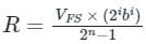
- The resolution of DAC is a change in analog voltage corresponding to the LSB bit increment at the input. The resolution (R) is calculated as:

where
N is the number of bits
VFs is the full scale deflection
Given
VFS = 5 V
N = 6
R =
= 78 mV
N is the number of bits
VFs is the full scale deflection
Given
VFS = 5 V
N = 6
R =
= 78 mV
The resolution of 4 Bit counting ADC is 05 V For an analog input 5.8 volt the output of ADC will be_____- a)1100
- b)1111
- c)1010
- d)1011
Correct answer is option 'A'. Can you explain this answer?
The resolution of 4 Bit counting ADC is 05 V For an analog input 5.8 volt the output of ADC will be_____
a)
1100
b)
1111
c)
1010
d)
1011
|
|
Sudhir Patel answered |
Concept:
- Analog-to-Digital Converters (ADCs) transform an analog voltage to a binary number (a series of 1’s and 0’s).
- Then eventually to a digital number (base 10) for reading on a meter, monitor, or chart.
- The ADC resolution depends upon the number of bits used to represent the digit number.
- As the number of bits increases the resolution of an Analog to Digital Converter improves and the quantization error decreases.
Resolution for n – bit A/D converter will be:
Where
R = Resolution
VFS is reference voltage 'or' Full-scale voltage
n = number of bits
2ibi gives output voltage value.
Calculation:
Given:
VFS = 5.8 V
n = 4
R = 05 V
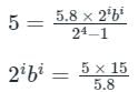
2ibi = 12.93 V ≈ 12 V
In bits, the output voltage will be 1100
Hence option (A) is the correct answer.
What is the main function of (A/D) or ADC converter?- a)Converts Digital to Analog Signal
- b)Converts Analog to Digital signal
- c)All of the mentioned
- d)None of the mentioned
Correct answer is option 'B'. Can you explain this answer?
What is the main function of (A/D) or ADC converter?
a)
Converts Digital to Analog Signal
b)
Converts Analog to Digital signal
c)
All of the mentioned
d)
None of the mentioned
|
|
Sneha Tiwari answered |
Introduction:
An A/D or ADC converter stands for Analog to Digital Converter. It is an electronic device that converts analog signals into digital signals. The main function of an ADC converter is to measure and convert continuous analog signals into discrete digital representations.
Key Points:
- ADC converter plays a crucial role in various applications such as data acquisition, control systems, communication systems, and many more.
- The conversion process involves two key steps: sampling and quantization.
- ADC converter quantizes the continuous analog signal by dividing it into discrete levels or steps.
- The input analog signal is sampled at regular intervals to obtain discrete data points.
- The sampled values are then quantized to a specific number of bits to represent the analog signal in digital form.
- The quantization process assigns a digital code to each sampled value based on the signal's amplitude.
- The output of the ADC converter is a binary code that represents the amplitude of the input analog signal.
- The converted digital signal can be easily processed, stored, transmitted, and manipulated by digital systems.
Advantages of ADC Converter:
- Accuracy: ADC converters provide accurate and precise measurements of analog signals.
- Digital Processing: The digitized signal can be easily processed using various digital signal processing techniques.
- Noise Immunity: Digital signals are less susceptible to noise and interference compared to analog signals.
- Compatibility: The digital output of the ADC converter can be easily interfaced with digital systems such as microcontrollers, computers, and other digital devices.
Applications of ADC Converter:
- Data Acquisition Systems: ADC converters are widely used in data acquisition systems to convert real-world analog signals into digital form for further processing and analysis.
- Communication Systems: In communication systems, ADC converters are used to convert analog voice signals into digital form for transmission over digital networks.
- Control Systems: ADC converters are used in control systems to measure analog sensor signals and convert them into digital form for controlling various processes and systems.
- Audio and Video Processing: ADC converters are used in audio and video processing applications to convert analog audio and video signals into digital form for editing, storage, and transmission.
Conclusion:
The main function of an ADC converter is to convert analog signals into digital form. It plays a crucial role in various applications and provides numerous advantages such as accuracy, digital processing capabilities, noise immunity, and compatibility with digital systems.
For a 12-bit ADC with voltage range 0-5 V, what will be the resolution?- a)2.44 mV
- b)0.416 mV
- c)2.4 mV
- d)1.22 mV
Correct answer is option 'D'. Can you explain this answer?
For a 12-bit ADC with voltage range 0-5 V, what will be the resolution?
a)
2.44 mV
b)
0.416 mV
c)
2.4 mV
d)
1.22 mV
|
|
Naina Agarwal answered |
Resolution of a 12-bit ADC:
The resolution of an ADC is determined by the number of bits it has. In this case, the ADC is 12-bit.
Calculation:
- The formula to calculate resolution is: Resolution = (Voltage Range) / (2^n), where n is the number of bits.
- Given that the voltage range is 0-5 V and the ADC is 12-bit, we can plug in the values and calculate the resolution.
- Resolution = 5 V / (2^12) = 5 V / 4096 = 0.00122 V = 1.22 mV
Therefore, the resolution of a 12-bit ADC with a voltage range of 0-5 V is 1.22 mV.
The full-scale output of a digital to analog converter is 20 mA. If the resolution is 80µA, then the minimum number of bits required and percentage resolution are:- a)8
- b)7
- c)3.9
- d)0.39
Correct answer is option 'D'. Can you explain this answer?
The full-scale output of a digital to analog converter is 20 mA. If the resolution is 80µA, then the minimum number of bits required and percentage resolution are:
a)
8
b)
7
c)
3.9
d)
0.39
|
|
Sudhir Patel answered |
Concept:
The resolution for n bit DAC is given by:

The % resolution for n bit DAC is given by:
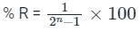
Calculation:
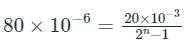
n = 8
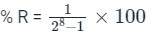
% R = 0.39
The difference between analog voltage represented by two adjacent digital codes of an analog to digital converter is- a)Accuracy
- b)Resolution
- c)Quantization
- d)Precision
Correct answer is option 'B'. Can you explain this answer?
The difference between analog voltage represented by two adjacent digital codes of an analog to digital converter is
a)
Accuracy
b)
Resolution
c)
Quantization
d)
Precision
|
|
Pragati Sengupta answered |
Resolution refers to the number of bits used to represent the analog voltage in the digital domain.
When an analog voltage is converted into a digital code by an Analog to Digital Converter (ADC), it is quantized into discrete levels based on the resolution of the ADC. The resolution determines the smallest change in voltage that can be represented by the ADC. Each additional bit in the digital code doubles the number of possible levels, thereby increasing the resolution.
Accuracy, on the other hand, refers to how close the converted digital code is to the actual analog voltage.
Accuracy is influenced by various factors such as linearity, offset error, gain error, and noise in the ADC. These factors can introduce errors in the conversion process, resulting in a deviation between the actual analog voltage and the digital code assigned to it.
Quantization is the process of mapping continuous analog values to discrete digital values.
When an analog voltage is converted to a digital code, it is quantized into a finite number of levels. This process introduces quantization error, which is the difference between the actual analog voltage and the nearest representable digital code. The quantization error is determined by the resolution of the ADC.
Precision refers to the level of detail or granularity in the representation of the analog voltage.
It is a measure of how closely spaced the digital codes are in relation to the actual analog voltage. Higher precision means smaller intervals between adjacent digital codes, allowing for more accurate representation of the analog signal.
In conclusion, the difference between the analog voltage represented by two adjacent digital codes of an ADC is the resolution. The resolution determines the smallest change in voltage that can be represented, and it directly affects the accuracy and precision of the conversion process. Higher resolution leads to better accuracy and precision in representing the analog voltage.
The advantage of using a dual slope ADC in a digital voltmeter is that- a)its accuracy is high
- b)its conversion time is small
- c)it gives output in BCD format
- d)it does not require a comparator
Correct answer is option 'A'. Can you explain this answer?
The advantage of using a dual slope ADC in a digital voltmeter is that
a)
its accuracy is high
b)
its conversion time is small
c)
it gives output in BCD format
d)
it does not require a comparator
|
|
Falak Desai answered |
Advantage of using a dual slope ADC in a digital voltmeter is that its accuracy is high.
Dual Slope ADC
A dual slope ADC is a type of analog-to-digital converter that uses the principle of integrating an unknown input voltage over a known period of time to produce a digital output. It is widely used in digital voltmeters due to its high accuracy.
Working Principle of Dual Slope ADC
The operation of a dual slope ADC involves two integration cycles: the positive slope integration and the negative slope integration.
1. Positive Slope Integration
- Initially, a counter is reset to zero and a known reference voltage of opposite polarity to the input voltage is applied.
- An integrator circuit starts integrating the unknown input voltage from zero towards the reference voltage.
- The integration process continues until the integrator output reaches zero.
2. Negative Slope Integration
- After the positive slope integration, the reference voltage is switched to the same polarity as the input voltage.
- The integrator circuit starts integrating the reference voltage from zero towards the input voltage.
- The integration process continues until the integrator output reaches zero.
Advantage of Dual Slope ADC in a Digital Voltmeter
1. High Accuracy:
- The main advantage of using a dual slope ADC in a digital voltmeter is its high accuracy.
- The dual slope integration technique eliminates many common sources of error found in other ADC architectures.
- It is less sensitive to noise, temperature variations, and component mismatch, resulting in higher accuracy measurements.
2. Noise Rejection:
- The dual slope ADC reduces the effect of noise by rejecting any noise signals during the integration process.
- As the integration time is long, the noise signals are effectively averaged out.
3. Linearity:
- The dual slope ADC exhibits excellent linearity due to its precise integration process.
- It provides a linear relationship between the input voltage and the digital output, enabling accurate voltage measurements.
4. Conversion Time:
- Although the conversion time of a dual slope ADC is longer compared to some other ADC types, it can still be fast enough for many applications.
- The conversion time mainly depends on the integration time for positive and negative slopes.
- With the use of high-speed operational amplifiers and accurate timing circuits, the conversion time can be minimized.
Conclusion
In conclusion, the advantage of using a dual slope ADC in a digital voltmeter is its high accuracy. The dual slope integration technique provides excellent noise rejection, linearity, and precision. Although the conversion time may be longer compared to some other ADC types, it can still be fast enough for many practical applications.
What is the resolution of a 0 - 5 V 8-bit DAC?- a)0.0019
- b)0.0039
- c)0.0078
- d)0.0156
Correct answer is option 'A'. Can you explain this answer?
What is the resolution of a 0 - 5 V 8-bit DAC?
a)
0.0019
b)
0.0039
c)
0.0078
d)
0.0156
|
|
Sudhir Patel answered |
Concept:
The resolution of either a digital-to-analog converter (DAC) or an analog-to-digital converter (ADC) is the measure of how finely its output may change between discrete, binary steps.
For an n-bit DAC, the resolution (R) is measured by:
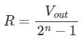
Vout = Output Voltage
n = number of bits
Calculation:
With Vout = 5 V, and n = 8 bits, the resolution will be:
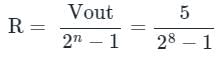
Resolution = 0.0196
Which of the following types of ADC is also known as continuous conversion type ADC?- a)Dual-slope ADC
- b)Counter-type ADC
- c)Tracking-type ADC
- d)Successive approximation ADC
Correct answer is option 'D'. Can you explain this answer?
Which of the following types of ADC is also known as continuous conversion type ADC?
a)
Dual-slope ADC
b)
Counter-type ADC
c)
Tracking-type ADC
d)
Successive approximation ADC
|
|
Imtiaz Ahmad answered |
A successive-approximation ADC is a type of analog-to-digital converter that converts a continuous analog waveform into a discrete digital representation using a binary search through all possible quantization levels before finally converging upon a digital output for each analog voltage conversion.
For an N-bit successive approximation ADC, the conversion time is
= N T
Where T is the time period of the clock pulse.
∴ The conversion time does not depend on the magnitude of the input voltage.
For an N-bit successive approximation ADC, the conversion time is
= N T
Where T is the time period of the clock pulse.
∴ The conversion time does not depend on the magnitude of the input voltage.
A signal channel signal acquisition system with 0-10 V range consist of a sample and hold circuit with worst case drop rate of 100 μV/ms and 10 bit ADC. The maximum conversion time for the ADC is- a)49 ms
- b)0.49 ms
- c)4.9 ms
- d)490 ms
Correct answer is option 'A'. Can you explain this answer?
A signal channel signal acquisition system with 0-10 V range consist of a sample and hold circuit with worst case drop rate of 100 μV/ms and 10 bit ADC. The maximum conversion time for the ADC is
a)
49 ms
b)
0.49 ms
c)
4.9 ms
d)
490 ms
|
|
Aman Mehra answered |
V/s. The system is connected to a 12-bit analog-to-digital converter (ADC) with a conversion time of 10 μs. The clock frequency of the ADC is 1 MHz.
To calculate the maximum allowable drop in voltage during the conversion time, we need to consider the worst case drop rate of the sample and hold circuit and the conversion time of the ADC.
The maximum allowable drop in voltage can be calculated using the formula:
Maximum Allowable Drop = Drop Rate * Conversion Time
Given that the drop rate is 100 V/s and the conversion time is 10 μs (or 10^-5 s), we can plug in these values into the formula:
Maximum Allowable Drop = 100 V/s * 10^-5 s
= 1 V
Therefore, the maximum allowable drop in voltage during the conversion time is 1 V.
Now, let's consider the clock frequency of the ADC, which is 1 MHz. This means that the ADC performs 1 million conversions per second.
Since the ADC has a 12-bit resolution, it can represent 2^12 = 4096 different voltage levels. Therefore, the voltage resolution of the ADC can be calculated as:
Voltage Resolution = (Voltage Range) / (Number of Levels)
= (10 V) / (4096)
≈ 0.00244 V
Therefore, the voltage resolution of the ADC is approximately 0.00244 V.
In summary, the signal acquisition system with a 0-10 V range can tolerate a maximum allowable drop in voltage of 1 V during the conversion time of the ADC. The ADC has a voltage resolution of approximately 0.00244 V.
A D/A converter has 5V full-scale input voltage and an accuracy of ± 0.2%. The maximum error for any output voltage will be- a)5 mV
- b)10 mV
- c)20 mV
- d)1 mV
Correct answer is option 'B'. Can you explain this answer?
A D/A converter has 5V full-scale input voltage and an accuracy of ± 0.2%. The maximum error for any output voltage will be
a)
5 mV
b)
10 mV
c)
20 mV
d)
1 mV
|
|
Anisha Bajaj answered |
0.1%. This means that the output voltage of the D/A converter will have a maximum error of 0.1% of the full-scale input voltage.
To calculate the maximum error, we can use the formula:
Maximum Error = Full-Scale Input Voltage * Accuracy
Maximum Error = 5V * 0.1% = 0.005V
Therefore, the D/A converter will have a maximum error of 0.005V.
To calculate the maximum error, we can use the formula:
Maximum Error = Full-Scale Input Voltage * Accuracy
Maximum Error = 5V * 0.1% = 0.005V
Therefore, the D/A converter will have a maximum error of 0.005V.
Maximum value of signal to noise ratio of an 8 bit ADC with an I/P range of 10 V will be- a)50 dB
- b)4
- c)8 dB3.48.9 dB
- d)49.8 dB
Correct answer is option 'D'. Can you explain this answer?
Maximum value of signal to noise ratio of an 8 bit ADC with an I/P range of 10 V will be
a)
50 dB
b)
4
c)
8 dB3.48.9 dB
d)
49.8 dB

|
Crack Gate answered |
Concept:
For an n-bit ADC signal to noise ratio is given by
= 1.8 + 6 n dB
Where message signal → sinusoidal & noise PDF = uniform distribution
Calculation:
Given data n = 8 bit
Signal to noise ratio (SNR) = 1.8 + 6 n dB
= 1.8 + 6 x 8
= 49.8 dB
The resolution of an 8 bit DAC will be:- a)1/255
- b)1/8
- c)1/128
- d)1/64
Correct answer is option 'A'. Can you explain this answer?
The resolution of an 8 bit DAC will be:
a)
1/255
b)
1/8
c)
1/128
d)
1/64
|
|
Imtiaz Ahmad answered |
Resolution: It is defined as the smallest change in the analog output voltage corresponding to a change of one bit in the digital input.
The percentage resolution (%R) of an n-bit DAC is:
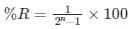
The resolution of an n-bit DAC with a range of output voltage from 0 to V is given by:
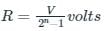
Calculation:
Number of bits (n) = 8
Resolution
The percentage resolution (%R) of an n-bit DAC is:
The resolution of an n-bit DAC with a range of output voltage from 0 to V is given by:
Calculation:
Number of bits (n) = 8
Resolution
What is the output of a digital to analog converter?- a)Smooth continuous wave
- b)Stairstep wave
- c)Triangular waves
- d)Circular waves
Correct answer is option 'B'. Can you explain this answer?
What is the output of a digital to analog converter?
a)
Smooth continuous wave
b)
Stairstep wave
c)
Triangular waves
d)
Circular waves
|
|
Sudhir Patel answered |
The Digital to analog converter takes the binary number as an input and produces the analog voltage proportional to the binary number. These analog voltages represent specific analog voltage levels and have stairstep characters.
The difference between analog voltage represented by two adjacent digital codes of an analog to digital converter is- a)Accuracy
- b)Resolution
- c)Quantization
- d)Precision
Correct answer is option 'B'. Can you explain this answer?
The difference between analog voltage represented by two adjacent digital codes of an analog to digital converter is
a)
Accuracy
b)
Resolution
c)
Quantization
d)
Precision
|
|
Starcoders answered |
Resolution: It is defined as the smallest change in the analog output voltage corresponding to a change of one bit in the digital output.
The percentage resolution (%R) of an n-bit DAC is:
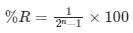
The resolution of an n-bit DAC with a range of output voltage from 0 to V is given by:
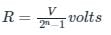
Hence the difference between analog voltage represented by two adjacent digital codes of an analog to digital converter is called resolution.
Hence option (2) is the correct answer.
The percentage resolution (%R) of an n-bit DAC is:
The resolution of an n-bit DAC with a range of output voltage from 0 to V is given by:
Hence the difference between analog voltage represented by two adjacent digital codes of an analog to digital converter is called resolution.
Hence option (2) is the correct answer.
What is the error that occurs when the number of bits is not sufficient enough to represent the analog voltages?- a)Data error
- b)Sampling error
- c)Acquisition error
- d)Quantization error
Correct answer is option 'D'. Can you explain this answer?
What is the error that occurs when the number of bits is not sufficient enough to represent the analog voltages?
a)
Data error
b)
Sampling error
c)
Acquisition error
d)
Quantization error
|
|
Sudhir Patel answered |
When the number of bits is not sufficient enough to represent the analog voltage levels, quantization error occurs. The greater the number of bits, the greater the number of increments over the analog range and the smaller the quantizing error.
The smallest change in the input signal that can be detected by an instrument is called- a)Accuracy
- b)Sensitivity
- c)Resolution
- d)Precision
Correct answer is option 'C'. Can you explain this answer?
The smallest change in the input signal that can be detected by an instrument is called
a)
Accuracy
b)
Sensitivity
c)
Resolution
d)
Precision
|
|
Starcoders answered |
- The smallest change in the input signal that can be detected by an instrument is referred to as its "resolution."
- The term resolution describes the finest detail that a device or system can detect or measure.
- It is a key parameter for systems that deal with digital signals, as it is directly linked to the quality or level of detail of the output.
What is the signal frequency if the rectangular digital wave has a time period of 71.4μs?- a)14,006Hz
- b)15,036Hz
- c)14Hz
- d)21,436Hz
Correct answer is option 'A'. Can you explain this answer?
What is the signal frequency if the rectangular digital wave has a time period of 71.4μs?
a)
14,006Hz
b)
15,036Hz
c)
14Hz
d)
21,436Hz
|
|
Sudhir Patel answered |
Signal frequency = 1/ time period of the wave = 1/71.4μs = 14,006Hz.
Chapter doubts & questions for Data Converters - Digital Circuits 2025 is part of Electronics and Communication Engineering (ECE) exam preparation. The chapters have been prepared according to the Electronics and Communication Engineering (ECE) exam syllabus. The Chapter doubts & questions, notes, tests & MCQs are made for Electronics and Communication Engineering (ECE) 2025 Exam. Find important definitions, questions, notes, meanings, examples, exercises, MCQs and online tests here.
Chapter doubts & questions of Data Converters - Digital Circuits in English & Hindi are available as part of Electronics and Communication Engineering (ECE) exam.
Download more important topics, notes, lectures and mock test series for Electronics and Communication Engineering (ECE) Exam by signing up for free.
Digital Circuits
76 videos|175 docs|70 tests
|
|
© EduRev
|
Education Revolution
|


|


Signup to see your scores
go up
within 7 days!
within 7 days!
Takes less than 10 seconds to signup