


All Exams >
UPSC >
Electrical Engineering Optional Notes for UPSC >
All Questions
All questions of Digital IC families (DTL, TTL, ECL, MOS, CMOS) for UPSC CSE Exam
CMOS logic families are associated with: - Low power dissipation
- High noise immunity
- Low Fan-out
- Comparatively high logic voltage swing
- a)1, 2 and 4 only
- b)1, 2 and 3 only
- c)2, 3 and 4 only
- d)1, 2, 3 and 4
Correct answer is option 'A'. Can you explain this answer?
CMOS logic families are associated with:
- Low power dissipation
- High noise immunity
- Low Fan-out
- Comparatively high logic voltage swing
a)
1, 2 and 4 only
b)
1, 2 and 3 only
c)
2, 3 and 4 only
d)
1, 2, 3 and 4
|
|
Ishan Chawla answered |
Overview of CMOS Logic Families
CMOS (Complementary Metal-Oxide-Semiconductor) logic families are widely used in digital circuits due to their advantageous characteristics. The question evaluates four specific attributes associated with CMOS technology.
1. Low Power Dissipation
- CMOS circuits consume power primarily during switching.
- In static state (no switching), they draw negligible power, making them ideal for battery-operated devices.
2. High Noise Immunity
- CMOS logic offers robust noise margins.
- This means it can tolerate variations in voltage levels without affecting functionality, enhancing reliability in noisy environments.
3. Low Fan-out
- Fan-out refers to the number of inputs that a single output can drive.
- CMOS can indeed have lower fan-out compared to other logic families, particularly in older technologies. However, modern CMOS can drive multiple inputs effectively.
4. Comparatively High Logic Voltage Swing
- CMOS logic levels are clearly defined, typically resulting in higher voltage swings compared to other families like TTL (Transistor-Transistor Logic).
- This characteristic also contributes to better noise margins.
Conclusion
Given these attributes, the correct answer is "a) 1, 2, and 4 only."
- 1 (Low Power Dissipation): True
- 2 (High Noise Immunity): True
- 3 (Low Fan-out): While true, it is not as defining for modern CMOS.
- 4 (Comparatively High Logic Voltage Swing): True
Thus, options 1, 2, and 4 align with the strengths of CMOS logic families, confirming the answer choice.

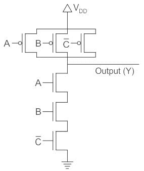
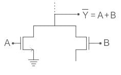
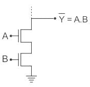
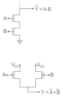
The output (Y) of the circuit shown in the figure is
- a)

- b)
- c)

- d)

Correct answer is option 'A'. Can you explain this answer?
The output (Y) of the circuit shown in the figure is
a)
b)
c)
d)

|
Pioneer Academy answered |
Concept:
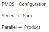
- The given circuit contains both NMOS and PMOS. So it is a CMOS implementation.
- For CMOS implementation if NMOS transistors are in series then PMOS transistors corresponding to their NMOS counterparts will be in parallel.
- Similarly, if NMOS transistors are in parallel then PMOS transistors corresponding to their NMOS counterparts will be in series.
- The output will be the negate of the function implemented by the NMOS transistors.
According to De morgan's theorem:
Calculation:
Calculation:
In the given circuit, signals A, B, and C̅ are in series for NMOS implementation. ∴ The output will be:
A digital CMOS IC operating at 10 MHz clock frequency consumes 100 mW power; the same IC operating at 15 MHz clock frequency consumes 140mW power. What is the static power consumption of the IC?- a)10 mW
- b)15 mW
- c)20 mW
- d)40 mW
Correct answer is option 'C'. Can you explain this answer?
A digital CMOS IC operating at 10 MHz clock frequency consumes 100 mW power; the same IC operating at 15 MHz clock frequency consumes 140mW power. What is the static power consumption of the IC?
a)
10 mW
b)
15 mW
c)
20 mW
d)
40 mW
|
|
Pooja Patel answered |
Concept:
Static power is proportional to the static current, i.e. the current that flows regardless of gate switching.
Dynamic Power is related to the current that flows when switching takes place and is given by for CMOS as:
Static power is proportional to the static current, i.e. the current that flows regardless of gate switching.
Dynamic Power is related to the current that flows when switching takes place and is given by for CMOS as:
P = fCV2cc
Or P = Kf (where K = Vcc2C)
Power consumed by CMOS = Pstatic + Pdynamic
Or P = Kf (where K = Vcc2C)
Power consumed by CMOS = Pstatic + Pdynamic
Calculation:
For f1 = 10MHz, Pconsumed = 100 mW = P1 (Let)
For f2 = 15MHz, Pconsumed = 140 mW = P2
⇒ P1 = Pstatic + Pdynamic
⇒ 100 mW = Pstatic + Kf1
⇒ 100 mW = Pstatic + K(10 M) …1)
Similarly, P2 = 140 mW = Pstatic + K(15 M) …2)
From equation (i) and (ii)
Pstatic = 20 mW
For f1 = 10MHz, Pconsumed = 100 mW = P1 (Let)
For f2 = 15MHz, Pconsumed = 140 mW = P2
⇒ P1 = Pstatic + Pdynamic
⇒ 100 mW = Pstatic + Kf1
⇒ 100 mW = Pstatic + K(10 M) …1)
Similarly, P2 = 140 mW = Pstatic + K(15 M) …2)
From equation (i) and (ii)
Pstatic = 20 mW
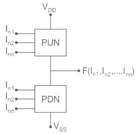
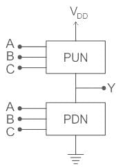
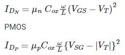
The circuit shown in the figure is:
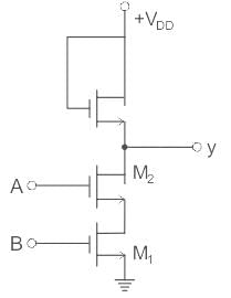
- a)OR gate
- b)NOR gate
- c)NAND gate
- d)AND gate
Correct answer is option 'C'. Can you explain this answer?
The circuit shown in the figure is:
a)
OR gate
b)
NOR gate
c)
NAND gate
d)
AND gate
|
|
Pooja Patel answered |
Concept:
MOS logic circuit consists of two network transistors, a pull-down network (PDN) and a Pull-up Network (PUN) as shown:
The PDN and PUN are connected in parallel to form OR logic function and they are connected in series to form AND logic as shown:
MOS logic circuit consists of two network transistors, a pull-down network (PDN) and a Pull-up Network (PUN) as shown:
The PDN and PUN are connected in parallel to form OR logic function and they are connected in series to form AND logic as shown:
In CMOS implementation of a NAND gate:- a)All the PMOS and NMOS are in series
- b)The two PMOS are in parallel and two NMOS are in series
- c)All the PMOS and NMOS are in parallel
- d)The two PMOS are in series and two NMOS are in parallel
Correct answer is option 'B'. Can you explain this answer?
In CMOS implementation of a NAND gate:
a)
All the PMOS and NMOS are in series
b)
The two PMOS are in parallel and two NMOS are in series
c)
All the PMOS and NMOS are in parallel
d)
The two PMOS are in series and two NMOS are in parallel
|
|
Rounak Rane answered |
Understanding CMOS NAND Gate Implementation
In a CMOS (Complementary Metal-Oxide-Semiconductor) NAND gate, the arrangement of PMOS and NMOS transistors is crucial for its functionality. Let's explore why option 'B' is the correct answer.
Configuration of PMOS and NMOS
- PMOS Transistors: In a NAND gate, two PMOS transistors are connected in parallel. This configuration allows for the output to be pulled high when at least one of the inputs is low.
- NMOS Transistors: Conversely, the two NMOS transistors are connected in series. This means that both NMOS transistors must be turned on for the output to be pulled low. This series connection ensures that the output is only low when both inputs are high.
Operation of the NAND Gate
- Input Low: If either input is low, at least one PMOS turns on, pulling the output high.
- Input High: If both inputs are high, both NMOS transistors turn on, connecting the output to ground and pulling it low.
Key Takeaways
- The arrangement of PMOS in parallel allows flexibility in switching to high, while NMOS in series ensures the output is low only under specific conditions.
- This complementary behavior of PMOS and NMOS is what gives the NAND gate its desired logic function.
In summary, the CMOS implementation of a NAND gate involves two PMOS transistors in parallel and two NMOS transistors in series, confirming that option 'B' is indeed correct. This design is efficient and plays a critical role in digital circuits.
The typical quiescent power dissipation of low-power CMOS units is- a)1 mW
- b)0.5 mW
- c)2 nW
- d)50 nW
Correct answer is option 'C'. Can you explain this answer?
The typical quiescent power dissipation of low-power CMOS units is
a)
1 mW
b)
0.5 mW
c)
2 nW
d)
50 nW
|
|
Pooja Patel answered |
- Complementary Metal-oxide-semiconductor (CMOS) uses complementary & symmetrical pair of P-type & n-type MOSFETS.
- The two important characteristics of CMOS devices are high noise immunity and low power dissipation.
- CMOS devices dissipate less power than NMOS devices because the CMOS dissipates power only when switching (“dynamic power), whereas N channel MOSFET dissipates power whenever the transistor is on because there is a current path from Vdd to Vss.
- In a CMOS, only one MOSFET is switched on at a time. Thus, there is no path from voltage source to ground so that a current can flow. Current flows in a MOSFET only during switching.
- Thus, compared to N-channel MOSFET has the advantage of lower drain current from the power supply, thereby causing less power dissipation.
- The typical quiescent power dissipation of low-power CMOS units is 2 nW
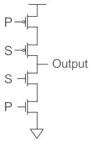
The above circuit acts as: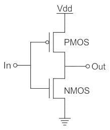
- a)Tristate buffer
- b)NAND gate
- c)Buffer
- d)Inverter
Correct answer is option 'D'. Can you explain this answer?
The above circuit acts as:
a)
Tristate buffer
b)
NAND gate
c)
Buffer
d)
Inverter
|
|
Pooja Patel answered |
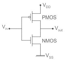
Inverter
- This is equal to NOT gate in the digital circuitry.
- The output of this is a compliment of the input.
This can be built from the transistors like BJT, MOSFET, etc…
The CMOS inverter consists of the NMOS and the PMOS field-effect transistors connected in one below the other.
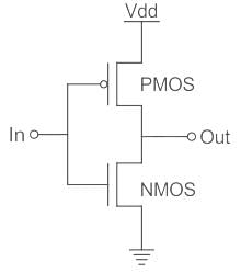
When In = Low
PMOS will be shorted and output will be High.
When In = High
NMOS will be shorted and output will be Low.
Hence it acts as an inverter.
PMOS will be shorted and output will be High.
When In = High
NMOS will be shorted and output will be Low.
Hence it acts as an inverter.
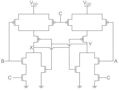
The following CMOS transistor based circuit with A, B, C as input and X, Y as output
- a)Positive edge triggered J-K flip flop
- b)Negative edge triggered J-K flip flop
- c)Positive edge trigger S-R flip flop
- d)None of the above
Correct answer is option 'C'. Can you explain this answer?
The following CMOS transistor based circuit with A, B, C as input and X, Y as output
a)
Positive edge triggered J-K flip flop
b)
Negative edge triggered J-K flip flop
c)
Positive edge trigger S-R flip flop
d)
None of the above
|
|
Pooja Patel answered |
C is the clock signal
Consider C = 1
The truth table is
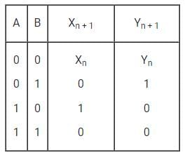
→ A = 1 and B = 1 is Forbidden
Whenever A = 1, Y = 0
Yn+1 = 0
Whenever B = 1, X = 0
XN+1 = 0
X = Q output
Y = Q̅ output
B = Reset (R)
A = Set (S)
Consider C = 1
The truth table is
→ A = 1 and B = 1 is Forbidden
Whenever A = 1, Y = 0
Yn+1 = 0
Whenever B = 1, X = 0
XN+1 = 0
X = Q output
Y = Q̅ output
B = Reset (R)
A = Set (S)
The full forms of the abbreviations TTL and CMOS in reference to logic families are- a)Triple Transistor Logic and Chip Metal Oxide Semiconductor
- b)Tristate Transistor Logic and Chip Metal Oxide Semiconductor
- c)Transistor Transistor Logic and Complementary Metal Oxide Semiconductor
- d)Tristate Transistor Logic and Complementary metal Oxide Silicon
Correct answer is option 'C'. Can you explain this answer?
The full forms of the abbreviations TTL and CMOS in reference to logic families are
a)
Triple Transistor Logic and Chip Metal Oxide Semiconductor
b)
Tristate Transistor Logic and Chip Metal Oxide Semiconductor
c)
Transistor Transistor Logic and Complementary Metal Oxide Semiconductor
d)
Tristate Transistor Logic and Complementary metal Oxide Silicon
|
|
Pooja Patel answered |
TTL stands for Transistor-Transistor Logic and CMOS stands for Complimentary Metal Oxide Semiconductor.
When there is no clock signal applied to CMOS logic circuits, they are referred to as- a)complex CMOS logic circuits
- b)static CMOS logic circuits
- c)NMOS transmission gates
- d)random PMOS logic circuit
Correct answer is option 'B'. Can you explain this answer?
When there is no clock signal applied to CMOS logic circuits, they are referred to as
a)
complex CMOS logic circuits
b)
static CMOS logic circuits
c)
NMOS transmission gates
d)
random PMOS logic circuit
|
|
Pioneer Academy answered |
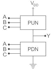
The circuit of a CMOS Logic circuit is as shown:
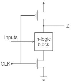
- It is a simple single dynamic CMOS with Precharge phase CLK = 0 and Evaluate phase CLK = 1.
- When no clock signal is applied, CMOS Logic circuit falls under static circuits in which every point in time, each gate output is connected to either VDD or VSS.
- A static CMOS logic circuit is a combination of two networks, called the pull-up-network (PUN) & pull-down-network (PDN) as shown:
The main advantage of CMOS is its- a)High power rating
- b)Small signal operation
- c)Switching capability
- d)Low power consumption
Correct answer is option 'D'. Can you explain this answer?
The main advantage of CMOS is its
a)
High power rating
b)
Small signal operation
c)
Switching capability
d)
Low power consumption
|
|
Pooja Patel answered |
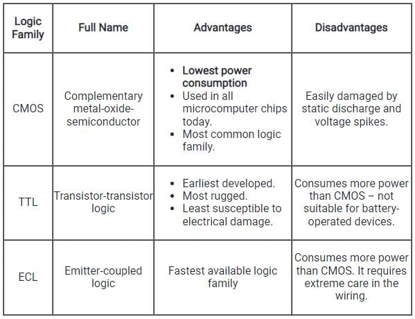
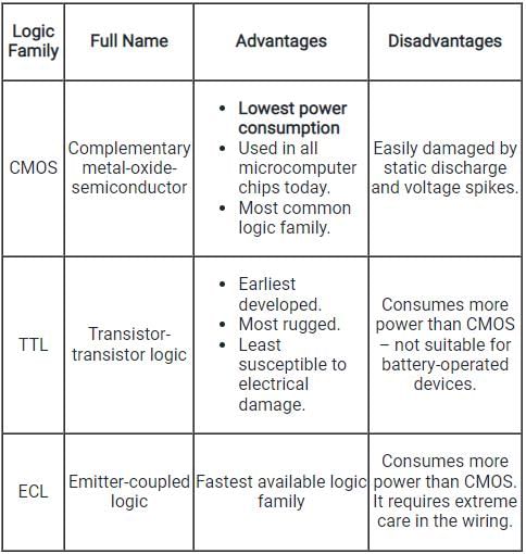
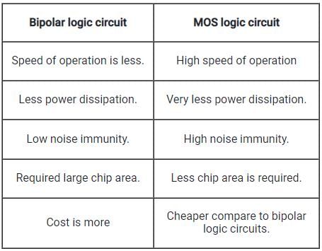
General comparison of three commonly available logic families is explained in the following table:
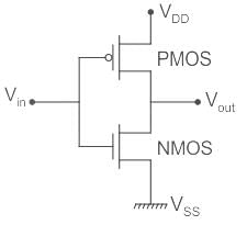
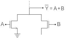
For the circuit shown in the figure, P and Q are the inputs and Y is the output.
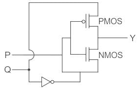 The logic implemented by the circuit is
- a)XNOR
- b)XOR
- c)NOR
- d)OR
Correct answer is option 'B'. Can you explain this answer?
For the circuit shown in the figure, P and Q are the inputs and Y is the output.
The logic implemented by the circuit is
a)
XNOR
b)
XOR
c)
NOR
d)
OR

|
Cstoppers Instructors answered |
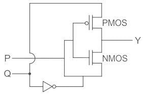
⇒ If P = high:
PMOS is OFF
NMOS is ON
then y = Q̅
⇒If P = low
PMOS is ON
NMOS is OFF
then y = Q
The truth table of the above will be as shown:
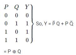
So, Ex – OR Operation is being performed.
PMOS is OFF
NMOS is ON
then y = Q̅
⇒If P = low
PMOS is ON
NMOS is OFF
then y = Q
The truth table of the above will be as shown:
So, Ex – OR Operation is being performed.
For a typical CMOS process, the minimum feature size is set to be 25 μm. The minimum line width at the process is set to be ______- a)100 μm
- b)12.5 μm
- c)50 μm
- d)25 μm
Correct answer is option 'C'. Can you explain this answer?
For a typical CMOS process, the minimum feature size is set to be 25 μm. The minimum line width at the process is set to be ______
a)
100 μm
b)
12.5 μm
c)
50 μm
d)
25 μm
|
|
Pioneer Academy answered |
Concept:
- Feature Size: The minimum feature size is the size or the width at which a transistor or any type of material on the silicon surface can be drawn at.
- If the minimum feature size can be reduced, this means that the transistor length can be reduced effectively making the transistor smaller with the same electrical properties.
- This allows for lower current flow between the junction for the same purpose and lesser heat dissipation.
The minimum line width is 2 × minimum feature size ---(1)
Calculation:
Given:
Minimum feature size = 25 μm
Now the minimum line width can be calculated from equation (1)
Minimum line width = 2 × 25 μm
Minimum line width = 50 μm
Hence option (3) is the correct answer.
Given:
Minimum feature size = 25 μm
Now the minimum line width can be calculated from equation (1)
Minimum line width = 2 × 25 μm
Minimum line width = 50 μm
Hence option (3) is the correct answer.
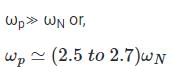
In the CMOS circuit shown, electron and hole mobilities are equal, and M1 and M2 are equally sized. The device M1 is in the linear region if
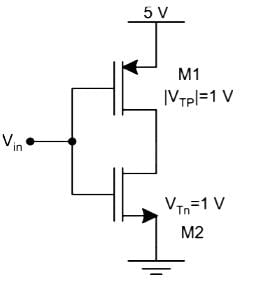
- a)Vin< 1.875 V
- b)1.875 V
- c)Vin> 3.125 V
- d)0
Correct answer is option 'A'. Can you explain this answer?
In the CMOS circuit shown, electron and hole mobilities are equal, and M1 and M2 are equally sized. The device M1 is in the linear region if
a)
Vin< 1.875 V
b)
1.875 V
c)
Vin> 3.125 V
d)
0
|
|
Pioneer Academy answered |
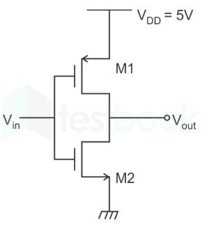
M1 will be in linear region if Vout>Vin + VT
At the edge of the linear region Vout= Vin + VT
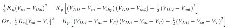
So, for Vin< 2.5 the PMOS will be in a linear region so the correct option is (1)
So, for Vin< 2.5 the PMOS will be in a linear region so the correct option is (1)
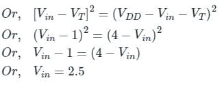
Output of the circuit shown below when S = 1 and S = 0 will be _____.
- a)P and High Impedance state respectively
- b)High Impedance state and P' respectively
- c)0 and 1 respectively
- d)X and P respectively
Correct answer is option 'B'. Can you explain this answer?
Output of the circuit shown below when S = 1 and S = 0 will be _____.
a)
P and High Impedance state respectively
b)
High Impedance state and P' respectively
c)
0 and 1 respectively
d)
X and P respectively
|
|
Pioneer Academy answered |
Concept:
Complementary Metal-oxide-semiconductor (CMOS) uses complementary & symmetrical pair of P-type & n-type MOSFETS.
Complementary Metal-oxide-semiconductor (CMOS) uses complementary & symmetrical pair of P-type & n-type MOSFETS.
- The two important characteristics of CMOS devices are high noise immunity and low power dissipation.
- In CMOS, during static operation at a time, only one MOS is ON i.e. either PMOS or NMOS. So there is no direct path from the power supply to the ground. Hence, Power dissipation in CMOS is low in static operation but it has high power dissipation in dynamic operation.
Calculation:
As the given figure is of CMOS with two inputs.
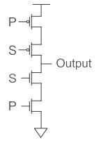
The upper part is PMOS which is switched on when 0 is applied and NMOS is switched on when 1 is applied.
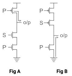
As the given figure is of CMOS with two inputs.
The upper part is PMOS which is switched on when 0 is applied and NMOS is switched on when 1 is applied.
- When S = 0 is applied, the PMOS connected to S (upper one) will be shorted and P at PMOS will appear across the output in complemented form as shown in fig(A).
So Output = P̅ - Now when S = 1 is applied, the NMOS connected to S (lower one) will be shorted, and due to which ground will appear across the output and the circuit will go in a high impedance state as shown in fig(B).
Hence option (2) is the correct answer.
The logic function f(X,Y) realized by the given circuit is
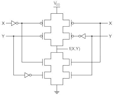
- a)NOR
- b)AND
- c)NAND
- d)XOR
Correct answer is option 'D'. Can you explain this answer?
The logic function f(X,Y) realized by the given circuit is
a)
NOR
b)
AND
c)
NAND
d)
XOR
|
|
Pioneer Academy answered |
Concept
CMOS logic circuit is an extension of a CMOS inverter. It consists of two network transistors, a pull-down network (PDN) constructed of an n-MOS and Pull-up Network (PUN) constructed of P-MOS.
PDN: Since nMOS conducts when the signal gate is high, PDN is activated when the inputs are high.
PUN: It comprises PMOS and conducts when the input signal gate is low.
The PDN and PUN are connected in parallel to form OR logic function and they are connected in series to form AND logic as shown:
In CMOS designs, why size of PMOS is kept larger than size of NMOS?- a)To get higher drive strength
- b)To reduce power dissipation
- c)To get balanced rise/fall time
- d)All of above
Correct answer is option 'C'. Can you explain this answer?
In CMOS designs, why size of PMOS is kept larger than size of NMOS?
a)
To get higher drive strength
b)
To reduce power dissipation
c)
To get balanced rise/fall time
d)
All of above
|
|
Pooja Patel answered |
To maximize the switching speed of a logic gate, for example, an inverter, it is best if the rise and fall time of the logic gate’s output signal is the same.
For this to occur, the top side transistors of the logic gate must switch current into the output of the logic gate at the same magnitude as the low side transistors.
Since PMOS transistors (high side) have approximately half the mobility of NMOS transistors (low side), it is necessary to add two parallel PMOS devices to the high side to achieve the equivalent magnitude currents.
In saturation
NMOS:
Cox and voltage are the same for both side, when

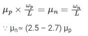
Considering the same length as it is a fixed constraint for the circuit.
that’s why we take PMOS size greater than N-MOS
NMOS:
Cox and voltage are the same for both side, when
Considering the same length as it is a fixed constraint for the circuit.
that’s why we take PMOS size greater than N-MOS
As compared to TTL, CMOS logic has- a)high speed of operation
- b)higher power dissipation
- c)smaller physical size
- d)none of the above
Correct answer is option 'C'. Can you explain this answer?
As compared to TTL, CMOS logic has
a)
high speed of operation
b)
higher power dissipation
c)
smaller physical size
d)
none of the above
|
|
Pooja Patel answered |
Option(1)- Schottky transistors are preferred for TTL logic systems. These transistors portray the Schottky effect and thus have higher switching speed in comparison to CMOS logic family.So option 1 is false.
Option(2)- TTL dissipates a lot of power where as CMOS uses almost no power in the static state (that is, when inputs are not changing). So option 2 is false.
Option(3)- TTL requires more space and isolation in comparison to CMOS logic family. The required silicon area for implementing CMOS is very small. So option 3 is true.
Which circuit takes the less chip area in large scale integration?- a)TTL logic circuits
- b)Bipolar circuits
- c)High power circuits
- d)CMOS circuits
Correct answer is option 'D'. Can you explain this answer?
Which circuit takes the less chip area in large scale integration?
a)
TTL logic circuits
b)
Bipolar circuits
c)
High power circuits
d)
CMOS circuits
|
|
Pooja Patel answered |
In large scale integration (LSI), CMOS (complementary Metal-oxide Semiconductor) circuit takes the less Chip area during fabrication. This is because the CMOS circuit is a combination of NMOS and PMOS and it is fabricated as a twin tub process where the required Chip area is less.
During the process of bipolar logic families (such as RTL, DTCL, DTL, HTL, TTL, and ECL) fabrication, required large chip area as these circuits consist of NPN and PNP transistor, diodes, resistors, etc.
Important Comparison between bipolar logic circuits and MOS logic circuits:
During the process of bipolar logic families (such as RTL, DTCL, DTL, HTL, TTL, and ECL) fabrication, required large chip area as these circuits consist of NPN and PNP transistor, diodes, resistors, etc.
Important Comparison between bipolar logic circuits and MOS logic circuits:
The CMOS circuit shown below implements the function
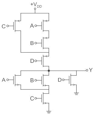
- a)(A + B) C + D
- b)
- c)
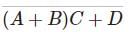
- d)(AB + C) D
Correct answer is option 'C'. Can you explain this answer?
The CMOS circuit shown below implements the function
a)
(A + B) C + D
b)
c)
d)
(AB + C) D
|
|
Pooja Patel answered |
Concept:
Calculation:
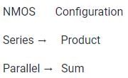
“We can get the answer either by using NMOS configuration OR by PMOS configuration”
Hence, we taking NMOS configuration:
∵ A and B is in parallel ⇒ A + B
A and B combinedly is in series with “C” ⇒ (A + B) C
A, B, C combinedly in parallel with “D” ⇒ (A + B) ⋅ C + D
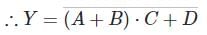
Hence, we taking NMOS configuration:
∵ A and B is in parallel ⇒ A + B
A and B combinedly is in series with “C” ⇒ (A + B) C
A, B, C combinedly in parallel with “D” ⇒ (A + B) ⋅ C + D
Chapter doubts & questions for Digital IC families (DTL, TTL, ECL, MOS, CMOS) - Electrical Engineering Optional Notes for UPSC 2025 is part of UPSC CSE exam preparation. The chapters have been prepared according to the UPSC CSE exam syllabus. The Chapter doubts & questions, notes, tests & MCQs are made for UPSC CSE 2025 Exam. Find important definitions, questions, notes, meanings, examples, exercises, MCQs and online tests here.
Chapter doubts & questions of Digital IC families (DTL, TTL, ECL, MOS, CMOS) - Electrical Engineering Optional Notes for UPSC in English & Hindi are available as part of UPSC CSE exam.
Download more important topics, notes, lectures and mock test series for UPSC CSE Exam by signing up for free.
Electrical Engineering Optional Notes for UPSC
550 videos|588 docs|343 tests
|
|
© EduRev
|
Education Revolution
|


|


Signup on EduRev and stay on top of your study goals
10M+ students crushing their study goals daily