


All Exams >
Electrical Engineering (EE) >
Analog and Digital Electronics >
All Questions
All questions of Combinational Logics for Electrical Engineering (EE) Exam
The output Y of a 2-bit comparator is logic 1 whenever the 2-bit input A is greater than the 2-bit input B. The number of combinations for which the output is logic 1, is- a)4
- b)6
- c)8
- d)10
Correct answer is option 'B'. Can you explain this answer?
The output Y of a 2-bit comparator is logic 1 whenever the 2-bit input A is greater than the 2-bit input B. The number of combinations for which the output is logic 1, is
a)
4
b)
6
c)
8
d)
10

|
Cstoppers Instructors answered |
The only possible combinations are
A = 01 and B = 0 0
A = 10 and B = 00, 01
A = 11 and B = 00, 01, 10
So there are only 6 combinations
Tips and Tricks:

where n = 2 bit
A = 01 and B = 0 0
A = 10 and B = 00, 01
A = 11 and B = 00, 01, 10
So there are only 6 combinations
Tips and Tricks:
where n = 2 bit


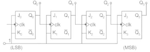
A Shift register in which the output of the last flip-flop is connected to the input of the first flip-flop- a)BCD counter
- b)Parallel counter
- c)Ripple counter
- d)Ring counter
Correct answer is option 'D'. Can you explain this answer?
A Shift register in which the output of the last flip-flop is connected to the input of the first flip-flop
a)
BCD counter
b)
Parallel counter
c)
Ripple counter
d)
Ring counter
|
|
Pooja Patel answered |
The Ring shift counter is a recirculating register in which the serial output is connected back to the serial input as shown:
A Straight ring counter with ‘n’ flip-flops will have n states.
Important Points
Johnson Counter:
A Straight ring counter with ‘n’ flip-flops will have n states.
Important Points
Johnson Counter:
A Johnson counter is a modified ring counter, where the inverted output from the last flip flop is connected to the input to the first.
The MOD of the Johnson counter is 2n if n flip-flops are used.
The circuit diagram for a 4-bit Johnson Counter is as shown:
Ripple Counter:
Ripple Counter:
A ripple counter is an asynchronous counter where only the first flip-flop is clocked by an external clock.
All subsequent flip-flops are clocked by the output of the preceding flip-flop
Parallel Counter:
Parallel Counter:
A parallel counter is a combinational logic circuit that receives a set of binary count signals in parallel and determines the final count after some fixed delay.
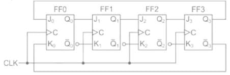
Which one of the following statements is true about the digital circuit shown in the figure?
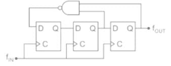
- a)It can be used for dividing the input frequency by 3.
- b)It can be used for dividing the input frequency by 5.
- c)It can be used for dividing the input frequency by 7.
- d)It cannot be reliably used as a frequency divider due to disjoint internal cycles.
Correct answer is option 'B'. Can you explain this answer?
Which one of the following statements is true about the digital circuit shown in the figure?
a)
It can be used for dividing the input frequency by 3.
b)
It can be used for dividing the input frequency by 5.
c)
It can be used for dividing the input frequency by 7.
d)
It cannot be reliably used as a frequency divider due to disjoint internal cycles.
|
|
Cstoppers Instructors answered |

From the given circuit diagram,
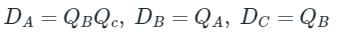
The output QA, QB, QC is repeating for every 5 clock pulses.
Hence frequency will be divided by 5.
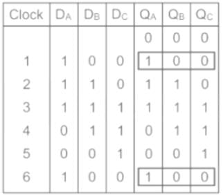
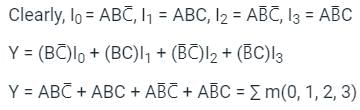
The logic function implemented by the following 4: 1 MUX is:
- a)Z = X and Y
- b)Z = X or Y
- c)Z = X XOR Y
- d)Z = X XNOR Y
Correct answer is option 'C'. Can you explain this answer?
The logic function implemented by the following 4: 1 MUX is:
a)
Z = X and Y
b)
Z = X or Y
c)
Z = X XOR Y
d)
Z = X XNOR Y
|
|
Pooja Patel answered |
Calculation:
For the given MUX, the output is given by,
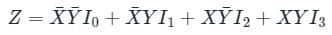
Given I0 = X, I1 = Y, I2 = X and I3 = 0

= X ⊕ Y (X-OR gate)
So, option (c)
Find the number of 2 × 1 MUX (multiplexers) required to implement 16 × 1 MUX.- a)15
- b)20
- c)5
- d)9
Correct answer is option 'A'. Can you explain this answer?
Find the number of 2 × 1 MUX (multiplexers) required to implement 16 × 1 MUX.
a)
15
b)
20
c)
5
d)
9
|
|
Mayank Sengupta answered |
It seems like you were cut off mid-sentence. Could you please provide more context or complete your question?
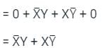
Minimum number of Half adders, Full adders, AND gates required to implement 2 × 3 multiplier is given as- a)1, 2, 6
- b)1, 1, 6
- c)2, 2, 6
- d)2, 1, 6
Correct answer is option 'D'. Can you explain this answer?
Minimum number of Half adders, Full adders, AND gates required to implement 2 × 3 multiplier is given as
a)
1, 2, 6
b)
1, 1, 6
c)
2, 2, 6
d)
2, 1, 6
|
|
Pooja Patel answered |
Explanation:
Multiplier
- A multiplier is a combinational logic circuit that we use to multiply binary digits.
- We use a multiplier in several digital signal processing applications.
- We use it to design calculators, mobiles, processors, and digital image processors.
Process
- The first product obtained from multiplying A0 with the multiplicand is called as partial product 1.
- And the second product obtained from multiplying A1 with the multiplicand is known as the partial product 2.
The structure of multiplication is explained below:
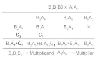
There are 6 product terms so to get all those 6 AND gates are required.
There are 6 product terms so to get all those 6 AND gates are required.
To get the addition of B1A0 and B0A1 we require one-half adder and this produces a carry also.
To get the addition of B2A0, B1A1 and C1 we require Full adder because of 3 inputs and this also produces a carry.
To get the B2A1 and C2 we require one-half adder because of 2 inputs.
Conclusion:
Total 6 AND gates, 2 Half adders and 1 Full adder are required.
A 4-bit synchronous counter uses flip-flops with a propagation delay time of 15 ns each. The maximum possible time required for change of state will be - a)15 ns
- b)30 ns
- c)60 ns
- d)none of the above
Correct answer is option 'A'. Can you explain this answer?
A 4-bit synchronous counter uses flip-flops with a propagation delay time of 15 ns each. The maximum possible time required for change of state will be
a)
15 ns
b)
30 ns
c)
60 ns
d)
none of the above
|
|
Pooja Patel answered |
Concept:
The maximum propagation delay (tpd) for the synchronous counter is given by:
tpd = td
td = Propagation delay of 1 Flip flop.
Calculation:
Given is a 4-bit synchronous counter for which the maximum possible time needed for the change of state will be the maximum possible propagation delay:
tpd = Delay of 1 flip-flop only
tpd = 15 ns
Important Points
Important Points
- In synchronous counters, all flip-flops change simultaneously and in asynchronous counters, the propagation delay of the flip-flops add up to produce the overall delay.
- Although synchronous counters usually have more combinational logic, the propagation delay through these gates is small compared to the propagation delay through many stages of flip-flops.
- So the Synchronous counter will provide the least delay compared to Asynchronous counters.
The maximum propagation delay for an n-bit asynchronous counter is given by:
tpd = n × td
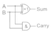
How many number of 2-input NAND gates are required to realise a half adder circuit?- a)5
- b)6
- c)4
- d)8
Correct answer is option 'A'. Can you explain this answer?
How many number of 2-input NAND gates are required to realise a half adder circuit?
a)
5
b)
6
c)
4
d)
8
|
|
Pooja Patel answered |
Half Adder using NAND Gates:
The half adder can also be designed with the help of NAND gates. NAND gate is considered as a universal gate. A universal gate can be used for designing any digital circuitry. It is always simple and efficient to use the minimum number of gates in the designing process of our circuit. The minimum number of NAND gates required to design a half adder is 5.
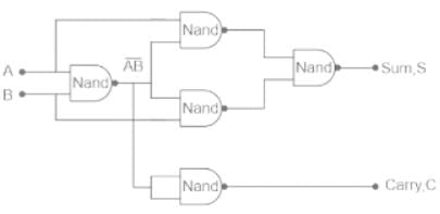
- The first NAND gate takes the inputs which are the two 1-bit numbers.
- The resultant NAND-operated inputs will be again given as input to 3- NAND gates along with the original input.
- Out of these 3 NAND gates, 2-NAND gates will generate the output which will be given as input to the NAND gate connected at the end.
- The gate connected at the end will generate the
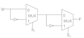
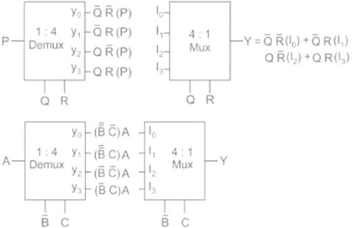
Consider the multiplexer based logic circuit shown in the figure.
Which one of the following Boolean functions is realized by the circuit?- a)
- b)F = WS1 + WS2 + S1S2
- c)
- d)F = W ⊕ S1 ⊕ S2
Correct answer is option 'D'. Can you explain this answer?
Consider the multiplexer based logic circuit shown in the figure.
Which one of the following Boolean functions is realized by the circuit?
Which one of the following Boolean functions is realized by the circuit?
a)
b)
F = WS1 + WS2 + S1S2
c)
d)
F = W ⊕ S1 ⊕ S2
|
|
Cstoppers Instructors answered |
Concept:
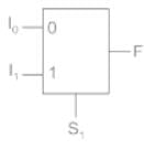
For a 2 × 1 MUX is shown above, the output function F is expressed as:
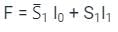
i.e. when S1 = 0, I0 is transmitted to the output.
For a 2 × 1 MUX is shown above, the output function F is expressed as:
i.e. when S1 = 0, I0 is transmitted to the output.
And when S1 = 1, I1 is transmitted to the output.
Application:
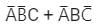
The given circuit is redrawn as:
Now, the required function f will be:
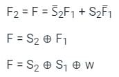
The given circuit is redrawn as:
Now, the required function f will be:
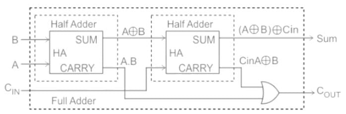
If A, B and C are the inputs of a full adder then the sum is given by __________- a)A AND B AND C
- b)A OR B AND C
- c)A XOR B XOR C
- d)A OR B OR C
Correct answer is option 'C'. Can you explain this answer?
If A, B and C are the inputs of a full adder then the sum is given by __________
a)
A AND B AND C
b)
A OR B AND C
c)
A XOR B XOR C
d)
A OR B OR C
|
|
Kalyan Patel answered |
Full Adder and its Inputs
A full adder is a combinational logic circuit that performs the addition of three bits. The three input bits of a full adder are A, B, and C (where C is the carry bit from the previous addition). The circuit adds the three bits and produces two outputs: Sum and Carry.
Sum Output of a Full Adder
The Sum output of a full adder is the result of adding the three input bits. The sum is calculated using the XOR (exclusive OR) gate. The XOR gate produces a 1 output when the inputs are different, and a 0 output when the inputs are the same. Therefore, the sum output of a full adder is given by:
Sum = A XOR B XOR C
Explanation:
- When A and B are different, the XOR gate produces a 1 output.
- If C is 1, then the XOR gate produces a 0 output because the carry bit is already included in the previous addition.
- If C is 0, then the XOR gate produces a 1 output because there is no carry bit to include in the addition.
- When A and B are the same, the XOR gate produces a 0 output.
- If C is 1, then the XOR gate produces a 1 output because the carry bit needs to be included in the addition.
- If C is 0, then the XOR gate produces a 0 output because there is no carry bit to include in the addition.
Therefore, the sum output of a full adder is given by A XOR B XOR C.
Conclusion
In conclusion, the sum output of a full adder is calculated using the XOR gate. The XOR gate produces a 1 output when the inputs are different, and a 0 output when the inputs are the same. Therefore, the sum output of a full adder is given by A XOR B XOR C.
A decoder converts n inputs to __________ outputs.- a)n
- b)n2
- c)2n
- d)nn
Correct answer is option 'C'. Can you explain this answer?
A decoder converts n inputs to __________ outputs.
a)
n
b)
n2
c)
2n
d)
nn
|
|
Srishti Choudhary answered |
Decoder in Digital Electronics:
Decoders are essential components in digital electronics that convert n inputs into 2^n outputs. In other words, a decoder takes a binary-coded input and activates one of its outputs based on the input combination.
Explanation:
- Number of Outputs: The number of outputs in a decoder is determined by the number of inputs it has. For n inputs, a decoder will have 2^n outputs. This is because each input line can have two possible states (0 or 1), leading to 2^n possible combinations.
- Binary to Decimal Conversion: Decoders are often used to convert binary information to decimal. For example, a 2-input decoder can be used to decode binary numbers 00, 01, 10, and 11 to corresponding decimal numbers 0, 1, 2, and 3.
- Addressing Multiple Devices: Decoders are also used in address decoding in memory and input/output devices. By using a decoder, a microprocessor can select a specific device or memory location based on the address provided.
- Applications: Decoders are widely used in various digital systems such as multiplexers, demultiplexers, memory systems, arithmetic logic units, etc. They play a crucial role in data processing and control operations.
Conclusion:
In summary, a decoder converts n inputs to 2^n outputs, making it a versatile and fundamental component in digital electronics. Understanding the working principles of decoders is essential for designing and implementing complex digital systems.
The addition of 3-bit is performed using which adder?- a)Counter
- b)Flip-flop
- c)Full adder
- d)Half adder
Correct answer is option 'C'. Can you explain this answer?
The addition of 3-bit is performed using which adder?
a)
Counter
b)
Flip-flop
c)
Full adder
d)
Half adder
|
|
Pooja Patel answered |
Half Adder: It is a logic circuit that performs addition on two binary digits. It produces a sum and carry.
Full Adder:
Full Adder:
- It is a logic circuit that takes three inputs to perform addition.
- Two binary input and one carry-in input of the previous stage is used.
- It generates sum and carry (C-out). C-in is a carry from a less significant digit and c-out is a carry from the most significant bit.
Additional Information
If we want to add two n- bit binary adders then it requires 1 half adder and n-1 full adder to complete the circuit. So, in the given question to add 4- bit binary numbers requires 1 half adder and 3 full adders.
How many OR gates are required for an octal-to-binary encoder?- a)3
- b)2
- c)8
- d)10
Correct answer is option 'A'. Can you explain this answer?
How many OR gates are required for an octal-to-binary encoder?
a)
3
b)
2
c)
8
d)
10
|
|
Ameya Nambiar answered |
**Octal-to-Binary Encoder**
An octal-to-binary encoder is a digital circuit that converts an octal input signal into a binary output signal. It takes in three inputs (A2, A1, A0) representing the octal number and produces four outputs (Y3, Y2, Y1, Y0) representing the binary number.
**Logic Diagram**
The logic diagram of an octal-to-binary encoder can be implemented using OR gates, as shown below:
```
_______
A2 --------| |
A1 --------| OR |------ Y3
A0 --------|_______|
_______
A2 --------| |
A1 --------| OR |------ Y2
A0 --------|_______|
_______
A2 --------| |
A1 --------| OR |------ Y1
A0 --------|_______|
_______
A2 --------| |
A1 --------| OR |------ Y0
A0 --------|_______|
```
**Explanation**
- The octal input signal has three bits (A2, A1, A0), representing the numbers 0 to 7.
- The binary output signal has four bits (Y3, Y2, Y1, Y0), representing the numbers 0 to 15.
- Each output bit is produced by a separate OR gate.
- The inputs A2, A1, and A0 are connected to each OR gate as shown in the logic diagram.
- The output of each OR gate will be high (1) if any of its inputs are high (1).
- Therefore, the OR gates perform a logical OR operation on the input bits and produce the corresponding output bits.
**Number of OR Gates**
To implement an octal-to-binary encoder, we need one OR gate for each output bit. Since there are four output bits (Y3, Y2, Y1, Y0), we need a total of four OR gates.
Hence, the correct answer is option A) 3.
How many 3 × 8 line decoders with an enable input line are needed to construct a 6 × 64 line decoder without using any other logic gate?- a)7
- b)8
- c)9
- d)10
Correct answer is option 'C'. Can you explain this answer?
How many 3 × 8 line decoders with an enable input line are needed to construct a 6 × 64 line decoder without using any other logic gate?
a)
7
b)
8
c)
9
d)
10
|
|
Pooja Patel answered |
Concept:
Decoder expansion
n1 × m1 → n2 × m2
D1 D2
Number of D2 decoder required = ∑ K
m2 / m1 = K1
K1 / m1 = K2
K2 / m1 = K3
⋮
Till 0 or 1
Calculation:
Given decoder 1 is 3 × 8 and the second decoder is 6 × 64
64 / 8 = 8
8 / 8 = 1
Number of 3 × 8 decoders = 8 + 1
Number of 3 × 8 decoders = 9
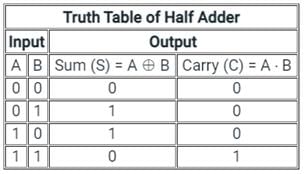
If A and B are the inputs of a half adder, the carry is given by __________- a)A AND B
- b)A OR B
- c)A XOR B
- d)A EX-NOR B
Correct answer is option 'A'. Can you explain this answer?
If A and B are the inputs of a half adder, the carry is given by __________
a)
A AND B
b)
A OR B
c)
A XOR B
d)
A EX-NOR B
|
|
Pallabi Pillai answered |
Half Adder:
A half adder is a logical circuit that adds two single-bit binary numbers A and B. It has two inputs, A and B, and two outputs, the sum (S) and the carry (C).
Inputs:
In a half adder, the inputs A and B represent the two bits that need to be added.
Carry:
The carry output of a half adder is a logic gate that determines if there is a carry generated when adding A and B together. It indicates whether there is a need to carry over to the next bit when adding multiple bits.
Logic Gates:
Logic gates are the fundamental building blocks of digital circuits. They perform logical operations on one or more binary inputs to produce a single binary output.
AND Gate:
An AND gate is a logic gate that outputs a 1 if and only if all of its inputs are 1. Otherwise, it outputs a 0. The truth table for an AND gate is as follows:
```
A | B | Output
--------------
0 | 0 | 0
0 | 1 | 0
1 | 0 | 0
1 | 1 | 1
```
Explanation:
In a half adder, the carry output is determined by the AND operation between the inputs A and B. The carry output is 1 only when both inputs A and B are 1, indicating that a carry is generated.
Let's consider the inputs A and B:
```
A | B
-----
0 | 0
0 | 1
1 | 0
1 | 1
```
When A and B are both 0, the carry output is 0. When A is 0 and B is 1, or A is 1 and B is 0, the carry output is also 0. However, when A and B are both 1, the carry output is 1.
Therefore, the carry output of a half adder is given by A AND B, which corresponds to option 'A'.
The logic shown in the given figure works as: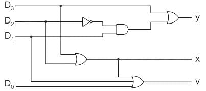
- a)decoder
- b)binary to XS-3 converter
- c)priority encoder
- d)binary to gray converter
Correct answer is option 'C'. Can you explain this answer?
The logic shown in the given figure works as:
a)
decoder
b)
binary to XS-3 converter
c)
priority encoder
d)
binary to gray converter
|
|
Pooja Patel answered |
Priority encoder:-
If more than one input is high then encoder produce an output which may not be correct to overcome this we use priority encoder.
We considered one more output, V in order to know, whether the code available at outputs is valid or not.
If at least one input of the encoder is ‘1’, then the code available at outputs is a valid one. In this case, the output, V will be equal to 1.
If all the inputs of encoder are ‘0’, then the code available at outputs is not a valid one. In this case, the output, V will be equal to 0.
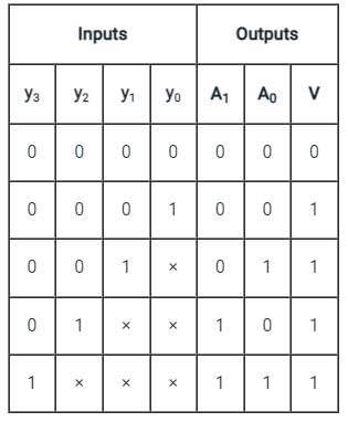
Analysis:-
Logic shown in given figure will work as
Priority encoder (4 × 2)
Inputs = D3, D2, D1, D0
Output:
y = D3 + D2’ D1
X = D3 + D2
V = D3 + D2 + D1 + D0
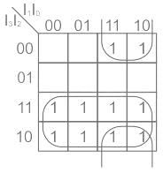
A 3 bit comparator circuit gives logic 1 output whenever the 3 bit input A is greater than the 3 bit input B. The output Boolean function y is represented by a K-map. The no. of 1 in the K-map is –- a)56
- b)28
- c)32
- d)24
Correct answer is option 'B'. Can you explain this answer?
A 3 bit comparator circuit gives logic 1 output whenever the 3 bit input A is greater than the 3 bit input B. The output Boolean function y is represented by a K-map. The no. of 1 in the K-map is –
a)
56
b)
28
c)
32
d)
24
|
|
Shanaya Mehta answered |
The number of 1's in the K-map depends on the values of inputs A and B. Without specific values for A and B, it is not possible to determine the number of 1's in the K-map.
The difference between half adder and full adder is __________- a)Half adder has two inputs while full adder has four inputs
- b)Half adder has one output while full adder has two outputs
- c)Half adder has two inputs while full adder has three inputs
- d)All of the Mentioned
Correct answer is option 'C'. Can you explain this answer?
The difference between half adder and full adder is __________
a)
Half adder has two inputs while full adder has four inputs
b)
Half adder has one output while full adder has two outputs
c)
Half adder has two inputs while full adder has three inputs
d)
All of the Mentioned
|
|
Pooja Patel answered |
Half adder has two inputs while full adder has three outputs; this is the difference between them, while both have two outputs SUM and CARRY.
If A and B are the inputs of a half adder, the sum is given by __________- a)A AND B
- b)A OR B
- c)A XOR B
- d)A EX-NOR B
Correct answer is option 'C'. Can you explain this answer?
If A and B are the inputs of a half adder, the sum is given by __________
a)
A AND B
b)
A OR B
c)
A XOR B
d)
A EX-NOR B
|
|
Dishani Bose answered |
Half Adder and its Inputs
A half adder is a digital circuit that is used to add two binary digits together. It has two inputs, A and B, and two outputs, sum and carry. The sum output gives the result of adding the two inputs, while the carry output indicates if there is a carry from the least significant bit to the most significant bit.
Logic Gates in Half Adder
The half adder uses two logic gates, an XOR gate and an AND gate, to perform the addition. The XOR gate gives a 1 output when one and only one of its inputs is 1. The AND gate gives a 1 output only when both of its inputs are 1.
Sum of Half Adder
To find the sum of the two binary digits using a half adder, we use the XOR gate. The sum output is the result of the XOR gate.
Sum Output
The sum output is given by the Boolean expression A XOR B. This means that if A and B are different, the sum output will be 1. If A and B are the same, the sum output will be 0.
Conclusion
Therefore, the sum output of a half adder is given by A XOR B. This is because we want the sum output to be 1 only when one of the inputs is 1, but not both. The XOR gate is the logic gate that satisfies this condition.
A _________ is a multiple-input, multiple-output logic circuit which converts coded inputs into coded outputs, where the input and output code are different.- a)decoder
- b)demultiplexer
- c)multiplexer
- d)encoder
Correct answer is option 'A'. Can you explain this answer?
A _________ is a multiple-input, multiple-output logic circuit which converts coded inputs into coded outputs, where the input and output code are different.
a)
decoder
b)
demultiplexer
c)
multiplexer
d)
encoder
|
|
Pooja Patel answered |
Encoder:
An encoder has 2n input lines and n output lines. In the encoder, the output lines generate the binary code corresponding to the input value which is active high.
Decoder:
It is a multi-input and multi-output logic circuit that converts coded inputs into coded outputs where input and output codes are different. Input code has fewer bits than output code. There is one to one mapping from input to output.
Multiplexer:
It is a digital switch. It allows digital information from several sources to be routed onto a single output line. A basic multiplexer has several data input lines and a single output line. The selection of a particular input line is controlled by selection lines. It is many to one mapping and provides the digital equivalent of an analog selector switch. Therefore it is the correct answer
Demultiplexer:
It is a circuit that receives information on a single line and transmits information on one of the 2n output lines. Selection of output line is controlled by values of n selection lines.
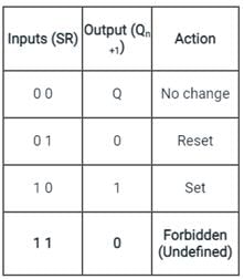
Identify the following sequential component.
- a)Master-slave flip flop
- b)Clocked flip flop
- c)J-K flip flop
- d)R-S flip flop
Correct answer is option 'D'. Can you explain this answer?
Identify the following sequential component.
a)
Master-slave flip flop
b)
Clocked flip flop
c)
J-K flip flop
d)
R-S flip flop
|
|
Pooja Patel answered |
Explanation:
The given sequential component is of RS Flip Flop.
Here A = R and B = S
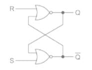
The truth table for the circuit is shown:
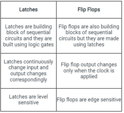
Important Points
The difference between latches and flip flops is shown
The truth table for the circuit is shown:
Important Points
The difference between latches and flip flops is shown
A __________ counter can be implemented using three flipflops.- a)mod-6
- b)mod-11
- c)mod-9
- d)mod-13
Correct answer is option 'A'. Can you explain this answer?
A __________ counter can be implemented using three flipflops.
a)
mod-6
b)
mod-11
c)
mod-9
d)
mod-13
|
|
Kritika Gupta answered |
Explanation:
In digital electronics, a counter is a sequential circuit that counts the number of occurrences of an event. A counter can be implemented using flip-flops, which are basic building blocks of sequential circuits.
Modulus Counter:
A modulus counter is a type of counter that counts up to a specific modulus value before resetting back to zero. In this case, we are looking for a counter that can count up to six before resetting.
Implementing a Mod-6 Counter:
To implement a mod-6 counter using flip-flops, we need to use three flip-flops. Each flip-flop will represent a binary digit, and the combination of these flip-flops will represent the count.
Binary Representation:
The modulus value can be represented in binary as 110, which means we need three bits to represent the count from 0 to 5.
Using D Flip-Flops:
D flip-flops are commonly used to implement counters. Each D flip-flop has two inputs - D (data) and CLK (clock). The output of one flip-flop is connected to the CLK input of the next flip-flop, creating a ripple effect.
Implementing a Mod-6 Counter using D Flip-Flops:
Here is how we can implement a mod-6 counter using three D flip-flops:
- Connect the Q output of the first flip-flop to the D input of the second flip-flop.
- Connect the Q output of the second flip-flop to the D input of the third flip-flop.
- Connect the Q output of the third flip-flop to the D input of the first flip-flop.
Working:
The counter starts at 000. On the rising edge of the clock signal, the first flip-flop increments its count by 1. When the count reaches 2 (010 in binary), the second flip-flop increments its count by 1. When the count reaches 4 (100 in binary), the third flip-flop increments its count by 1.
Reset:
When the count reaches 6 (110 in binary), the counter resets back to 000 and starts counting again. This creates a mod-6 counter.
Conclusion:
Therefore, a mod-6 counter can be implemented using three flip-flops.
A mod–n counter using a synchronous binary up–counter with synchronous clear input is shown in the figure. The value of n is_________. (Important - Enter only the numerical value in the answer)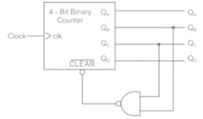 Correct answer is '7'. Can you explain this answer?
A mod–n counter using a synchronous binary up–counter with synchronous clear input is shown in the figure. The value of n is_________.
(Important - Enter only the numerical value in the answer)
|
|
Cstoppers Instructors answered |
Concept:
CLR: It is an active low signal. It is activated when CLR = 0 and it resets the FF.
CLR: It is an active high signal. It is activated when CLR = 1 and it Resets the FF.
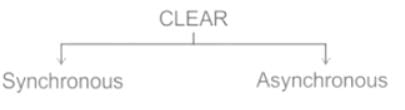
Synchronous: Synchronous clear is synchronized with the clock. It waits for a clock pulse to Reset FF output.
Synchronous: Synchronous clear is synchronized with the clock. It waits for a clock pulse to Reset FF output.
Asynchronous: Asynchronous Clear is not synchronized with the clock. It does not wait for a clock pulse to Reset FF output.
Application:
From given sequential circuit:
CLR = QB ⋅ QC
When both QB & QC equal to 1 then CLR = 0. Otherwise CLR = 1
Now,
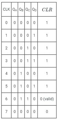
Since it is given that the counter have synchronous clear input, the output of the counter will reset at the 7th clock pulse.
Since it is given that the counter have synchronous clear input, the output of the counter will reset at the 7th clock pulse.
∴ The mod of the counter, n = 7
A full adder combinational circuit has- a)3 inputs and 2 outputs
- b)2 inputs and 0 outputs
- c)1 input and 0 output
- d)4 inputs and 1 output
Correct answer is option 'A'. Can you explain this answer?
A full adder combinational circuit has
a)
3 inputs and 2 outputs
b)
2 inputs and 0 outputs
c)
1 input and 0 output
d)
4 inputs and 1 output
|
|
Manoj Mehra answered |
Understanding Full Adder Circuits
A full adder is a crucial component in digital electronics, used for binary addition. Let's break down its characteristics:
Inputs of a Full Adder
- A full adder requires three inputs:
- Two inputs represent the bits to be added (let's call them A and B).
- One input is the carry-in (C_in) from a previous less significant bit addition.
Outputs of a Full Adder
- The full adder produces two outputs:
- The sum output (S) results from the addition of the input bits and the carry-in.
- The carry-out (C_out) indicates if there is a carry that needs to be added to the next more significant bit.
Functionality of a Full Adder
- The full adder operates based on the following logic:
- The sum (S) can be calculated as: S = A XOR B XOR C_in.
- The carry-out (C_out) can be calculated as: C_out = (A AND B) OR (C_in AND (A XOR B)).
Conclusion
In summary, a full adder indeed has three inputs and two outputs. It plays a vital role in arithmetic operations within digital circuits, especially in constructing arithmetic logic units (ALUs) and adding circuits. Option 'A' is correct as it accurately reflects the input-output configuration of a full adder.
Circuit for comparing 2 n-bit numbers has ____ entries in truth table- a)2n
- b)n
- c)22n
- d)2n
Correct answer is option 'C'. Can you explain this answer?
Circuit for comparing 2 n-bit numbers has ____ entries in truth table
a)
2n
b)
n
c)
22n
d)
2n
|
|
Gargi Basak answered |
Introduction:
A circuit for comparing two n-bit numbers is used to determine the relationship between the two numbers. It compares each corresponding bit of the two numbers and generates an output based on the result of the comparison. The truth table of this circuit represents all possible input combinations and their corresponding outputs.
Explanation:
To determine the number of entries in the truth table for a circuit comparing two n-bit numbers, we need to consider the total number of possible input combinations.
Number of Bits:
Let's assume that we have two n-bit numbers, A and B. Each number has n bits, where the most significant bit (MSB) is bit n-1 and the least significant bit (LSB) is bit 0.
Number of Input Combinations:
For each bit, there are two possible values, 0 or 1. Therefore, the total number of possible input combinations is given by 2^n for both numbers. As there are two numbers being compared, the total number of input combinations for the truth table can be calculated as (2^n) x (2^n).
Number of Entries in Truth Table:
The truth table consists of all possible input combinations and their corresponding outputs. Each input combination represents a row in the truth table, and the number of rows is equal to the number of entries in the truth table.
Since there are (2^n) x (2^n) possible input combinations, the truth table for the circuit comparing two n-bit numbers will have (2^n) x (2^n) entries.
Answer:
Therefore, the correct answer is option 'C', which states that the circuit for comparing two n-bit numbers has (2^n) x (2^n) entries in the truth table.
Summary:
- A circuit for comparing two n-bit numbers is used to determine the relationship between the two numbers.
- The truth table of this circuit represents all possible input combinations and their corresponding outputs.
- The number of entries in the truth table is equal to the total number of possible input combinations.
- For two n-bit numbers, the total number of input combinations is given by (2^n) x (2^n).
- Hence, the circuit for comparing two n-bit numbers has (2^n) x (2^n) entries in the truth table.
For the following cascaded Counters find the value of X of the mode-X counter. (Important - Enter only the numerical value in the answer)
Correct answer is '10'. Can you explain this answer?
For the following cascaded Counters find the value of X of the mode-X counter.
(Important - Enter only the numerical value in the answer)

|
Pioneer Academy answered |
Concept:
- The N-bit ring counter will have total N states/Mods.
- The N-bit johnson counter will have a total 2N number of states/Mods.
- The output frequency of a counter is the input frequency divided by the mode number of that counter.
Solution:
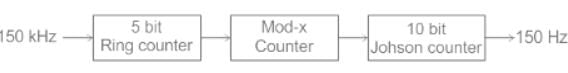
The frequency at node Y is
The frequency at node Y is
Fy = 150kHz/5
= 30 kHz
The frequency at node Z is
Fz = 30kHz/X
here X is the Mod number
then output frequency is given by
∴ X = 10
In which operation carry is obtained?- a)Subtraction
- b)Addition
- c)Multiplication
- d)Both addition and subtraction
Correct answer is option 'B'. Can you explain this answer?
In which operation carry is obtained?
a)
Subtraction
b)
Addition
c)
Multiplication
d)
Both addition and subtraction
|
|
Tarun Chawla answered |
Obtaining Carry in Addition
When performing addition, the carry is obtained when the sum of two digits in a particular position exceeds the base of the number system being used. For example, when adding two binary numbers, if the sum of two bits in the same position is 2 (10 in binary), a carry of 1 is generated and added to the next higher position.
Example:
1101
+ 1011
-------
10000
In this example, when adding the rightmost bits (1 + 1), the sum is 10, which results in a carry of 1 to the next higher position.
Carry in Subtraction
In subtraction, the concept of borrowing is used instead of carrying. When subtracting a larger digit from a smaller one, borrowing is required to perform the operation.
Example:
1011
- 0110
--------
001
In this example, when subtracting the second digit from the first digit, borrowing is needed to perform the subtraction operation.
Conclusion
In the operation of addition, the carry is obtained when the sum of two digits exceeds the base of the number system. In contrast, borrowing is used in subtraction when subtracting a larger digit from a smaller one. Therefore, carry is obtained in the addition operation.


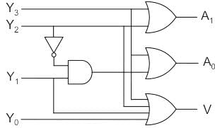
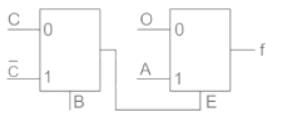
The Boolean function ‘f’ implemented as shown in the figure using two input multiplexers is:
- a)
- b)

- c)

- d)
Correct answer is option 'A'. Can you explain this answer?
The Boolean function ‘f’ implemented as shown in the figure using two input multiplexers is:
a)
b)
c)
d)
|
|
Luminary Institute answered |
Concept:
For a 2 × 1 MUX is shown above, the output function F is expressed as:
i.e. when S1 = 0, I0 is transmitted to the output.
For a 2 × 1 MUX is shown above, the output function F is expressed as:
i.e. when S1 = 0, I0 is transmitted to the output.
And when S1 = 1, I1 is transmitted to the output.
Application:
The output of the 1st MUX will be:
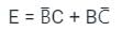
The final output will be:
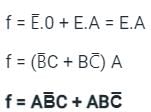
The final output will be:
An eight-bit binary ripple UP counter with a modulus of 256 is holding the count 01111111. What will be the count after 135 clock pulses?- a)0000 0101
- b)1111 1001
- c)0000 0110
- d)0000 0111
Correct answer is option 'C'. Can you explain this answer?
An eight-bit binary ripple UP counter with a modulus of 256 is holding the count 01111111. What will be the count after 135 clock pulses?
a)
0000 0101
b)
1111 1001
c)
0000 0110
d)
0000 0111
|
|
Pooja Patel answered |
01111111 → 127
After 135 clock cycles, we will get
127 + 135 = 262
∴ The total number of clock pulses will be 262
As the modulus is 256,
After 256 clock pulses, the sequence will repeat.
262 = 256 + 6
∴ 00 00 00 00
257 → 00 00 00 01
258 → 00 00 00 10
259 → 00 00 00 11
260 → 00 00 01 00
261 → 00 00 01 01
262 → 00 00 01 10
If the input to a T flip-flop is a 100 MHz signal, the final output of three T flip-flops in a cascade is- a)1000 MHz
- b)520 MHz
- c)333 MHz
- d)12.5 MHz
Correct answer is option 'D'. Can you explain this answer?
If the input to a T flip-flop is a 100 MHz signal, the final output of three T flip-flops in a cascade is
a)
1000 MHz
b)
520 MHz
c)
333 MHz
d)
12.5 MHz
|
|
Pankaj Mehta answered |
Explanation:
To understand why the final output of three T flip-flops in a cascade is 12.5 MHz, let's first understand what a T flip-flop does and how it works.
T Flip-Flop:
A T flip-flop is a type of flip-flop that toggles its output based on the input signal. The input to a T flip-flop is called the "toggle" input, and it can either be a logic high (1) or a logic low (0). When the toggle input is high (1), the output of the flip-flop toggles between its current state and its complemented state. When the toggle input is low (0), the output remains unchanged.
Cascade Connection:
When multiple flip-flops are connected in cascade, the output of one flip-flop becomes the input to the next flip-flop. In this case, we have three T flip-flops connected in cascade.
Frequency Division:
Each T flip-flop in the cascade divides the input frequency by two. This means that the output frequency of the first flip-flop is half of the input frequency, the output frequency of the second flip-flop is half of the output frequency of the first flip-flop, and so on.
Calculating the Output Frequency:
Given that the input frequency is 100 MHz, let's calculate the output frequency of the cascade.
- The output frequency of the first flip-flop is half of the input frequency, which is 100 MHz / 2 = 50 MHz.
- The output frequency of the second flip-flop is half of the output frequency of the first flip-flop, which is 50 MHz / 2 = 25 MHz.
- The output frequency of the third flip-flop is half of the output frequency of the second flip-flop, which is 25 MHz / 2 = 12.5 MHz.
Therefore, the final output of the three T flip-flops in a cascade is 12.5 MHz.
Conclusion:
The final output of three T flip-flops in a cascade, when the input is a 100 MHz signal, is 12.5 MHz. This is because each flip-flop divides the frequency by two, resulting in a progressive reduction of the frequency as it passes through each flip-flop.
How many AND, OR and EXOR gates are required for the configuration of full adder?- a)1, 2, 2
- b)2, 1, 2
- c)3, 1, 2
- d)4, 0, 1
Correct answer is option 'B'. Can you explain this answer?
How many AND, OR and EXOR gates are required for the configuration of full adder?
a)
1, 2, 2
b)
2, 1, 2
c)
3, 1, 2
d)
4, 0, 1
|
|
Ankita Das answered |
Full Adder Configuration
To understand the number of gates required for the configuration of a full adder, let's first discuss what a full adder is and its logical representation.
A full adder is a combinational circuit that takes in three inputs: A, B, and Cin (carry-in) and produces two outputs: Sum (S) and Cout (carry-out). It is used to add two binary numbers along with a carry input from the previous stage.
The logical representation of a full adder can be expressed using basic logic gates such as AND, OR, and EXOR gates.
Logical Representation of Full Adder
The logical representation of a full adder is as follows:
1. Sum (S) output:
- It is the output of the EXOR gate.
- It is calculated by taking the EXOR of A, B, and Cin.
2. Carry-out (Cout) output:
- It is the output of the OR gate.
- It is calculated by taking the OR of the AND gates' outputs.
Calculating the Number of Gates
Now, let's calculate the number of AND, OR, and EXOR gates required for the configuration of a full adder.
1. AND gates:
- We require 2 AND gates to calculate the carry-out (Cout) output.
- Each AND gate takes 2 inputs, so a total of 2 AND gates are needed.
2. OR gates:
- We require 1 OR gate to calculate the carry-out (Cout) output.
- The OR gate takes 2 inputs.
3. EXOR gates:
- We require 2 EXOR gates to calculate the sum (S) output.
- Each EXOR gate takes 3 inputs, so a total of 2 EXOR gates are needed.
Hence, the number of AND, OR, and EXOR gates required for the configuration of a full adder is as follows:
- AND gates: 2
- OR gates: 1
- EXOR gates: 2
Therefore, the correct answer is option 'B' (2, 1, 2).
Which of the following can be represented for decoder?- a)Sequential circuit
- b)Combinational circuit
- c)Logical circuit
- d)None of the mentioned
Correct answer is option 'B'. Can you explain this answer?
Which of the following can be represented for decoder?
a)
Sequential circuit
b)
Combinational circuit
c)
Logical circuit
d)
None of the mentioned
|
|
Yashvi Shah answered |
Decoder:
A decoder is a digital circuit that converts coded input signals into a specific set of output signals. It is used in various applications such as data decoding, address decoding, and memory decoding. The main function of a decoder is to select one of the many outputs based on the input code.
Combinational Circuit:
A combinational circuit is a digital circuit that produces an output based on the current input values. It does not have any memory elements, and the output is solely determined by the current input values. Combinational circuits are designed using logic gates such as AND, OR, NOT, etc.
Sequential Circuit:
A sequential circuit is a digital circuit that has memory elements such as flip-flops. The output of a sequential circuit depends not only on the current input values but also on the previous input values and the state of the memory elements. Sequential circuits have a clock signal that controls the timing of their operation.
Logical Circuit:
A logical circuit refers to any circuit that performs logical operations such as AND, OR, NOT, etc. Both combinational and sequential circuits can be considered as logical circuits since they involve logical operations.
Representation for Decoder:
A decoder is a combinational circuit. It takes an n-bit input and produces 2^n outputs. Each output corresponds to a unique input combination. The number of outputs is determined by the number of input lines. For example, a 2-to-4 decoder has 2 input lines and produces 4 output lines.
A decoder can be represented using logic gates such as AND gates and NOT gates. The input lines are connected to the inputs of the AND gates, and their outputs are connected to the output lines. The output lines are activated based on the specific input combination. For example, if the input code is '00', the first output line is activated. If the input code is '01', the second output line is activated, and so on.
Since a decoder does not have any memory elements and its output is solely determined by the input code, it is considered as a combinational circuit. It does not depend on any previous input values or memory states. Therefore, the correct answer is option 'B' - Combinational circuit.
Consider the output A and B with I0, I1, I2 and I3 as input and ‘A’ and ‘B’ as output,A = I2 + I3B = I̅2 I1 + I3The above circuit is:- a)4:1 multiplexer
- b)De-multiplexer
- c)BCD circuit
- d)Priority Encoder
Correct answer is option 'D'. Can you explain this answer?
Consider the output A and B with I0, I1, I2 and I3 as input and ‘A’ and ‘B’ as output,
A = I2 + I3
B = I̅2 I1 + I3
The above circuit is:
a)
4:1 multiplexer
b)
De-multiplexer
c)
BCD circuit
d)
Priority Encoder
|
|
Pooja Patel answered |
A 4 to 2 Priority Encoder takes 4 input bits and produces 2 Output bits. The truth Table of a 4 to 2 Priority Encoder is as shown:
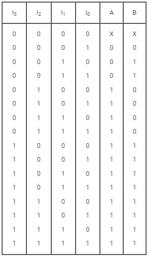
We use Karnaugh Map to minimize the logic for B as shown:
B = I̅2I1 + I3
Similarly the expression for A in obtained using K-map as shown:
A = I2 + I3
So, the given circuit is a priority Encoder only.
Which of the following is not a sequential circuit?- a)flip-flop
- b)counter
- c)shift register
- d)multiplexer
Correct answer is option 'D'. Can you explain this answer?
Which of the following is not a sequential circuit?
a)
flip-flop
b)
counter
c)
shift register
d)
multiplexer
|
|
Rajesh Saha answered |
Sequential Circuit
A sequential circuit is a digital circuit that has memory. It means the output of the circuit depends not only on the present input but also on the past input. The sequential circuits can be classified into two categories: Synchronous and Asynchronous circuits.
Synchronous circuits are the circuits that use clocks to synchronize the input and output signals. The input signals are sampled at the rising or falling edge of the clock, and the output signals are updated accordingly. Flip-flops, counters, and shift registers are examples of synchronous circuits.
Asynchronous circuits are the circuits that do not use clocks to synchronize the input and output signals. The output signals are updated whenever the input signals change. Asynchronous circuits are slower and more complex than synchronous circuits.
The Answer
The correct answer to the given question is option 'D', i.e., Multiplexer. A multiplexer is a combinational circuit that selects one input signal out of multiple input signals based on the control signals. A multiplexer does not have any memory or feedback, so it is not a sequential circuit.
Conclusion
In conclusion, a sequential circuit is a digital circuit that has memory, and the output depends on the present and past input signals. Synchronous and asynchronous circuits are two categories of sequential circuits. Flip-flops, counters, and shift registers are examples of synchronous circuits, while multiplexers are not sequential circuits.
Which of the following is a decoder IC?- a)7890
- b)8870
- c)4047
- d)4041
Correct answer is option 'B'. Can you explain this answer?
Which of the following is a decoder IC?
a)
7890
b)
8870
c)
4047
d)
4041
|
|
Pooja Patel answered |
8870 is a DTMF decoder circuit, which decodes DTMF tune and produces corresponding output.
Identify the 1 – bit comparator circuit
- a)

- b)

- c)

- d)

Correct answer is option 'A'. Can you explain this answer?
Identify the 1 – bit comparator circuit
a)
b)
c)
d)
|
|
Pioneer Academy answered |
Comparator:
A comparator is a combinational circuit that gives the output in terms of input signals.
It is used to compare numbers and represent their relationship with each other.
It compares the signals as A > B, A < B, and A = B.
1-bit comparator:
A 1-bit comparator circuit is shown below.
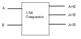
In this circuit, we can compare two input signals
The truth table for the 1-bit comparator is
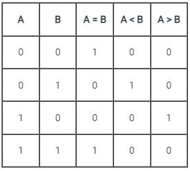
The expression for A = B: A ⊙ B
The expression for A > B: A B̅
The expression for A < B: A̅ B
A comparator is a combinational circuit that gives the output in terms of input signals.
It is used to compare numbers and represent their relationship with each other.
It compares the signals as A > B, A < B, and A = B.
1-bit comparator:
A 1-bit comparator circuit is shown below.
In this circuit, we can compare two input signals
The truth table for the 1-bit comparator is
The expression for A = B: A ⊙ B
The expression for A > B: A B̅
The expression for A < B: A̅ B
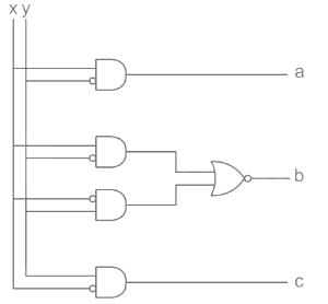
The circuit shown in the figure is a –
- a)Adder
- b)Comparator
- c)Subtractor
- d)Parity generator
Correct answer is option 'B'. Can you explain this answer?
The circuit shown in the figure is a –
a)
Adder
b)
Comparator
c)
Subtractor
d)
Parity generator
|
|
Cstoppers Instructors answered |
From the given circuit we can find the outputs expression as follows:
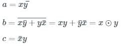
Now, we can observe that
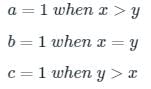
So, the given circuit in question behaves like a comparator circuit.
Now, we can observe that
So, the given circuit in question behaves like a comparator circuit.
A digital circuit which compares two numbers A3 A2 A1 A0, B3 B2 B1 B0 is shown in figure. To get output Y = 1, the correct pair of input numbers are
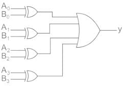
- a)1010, 1010
- b)0101, 0101
- c)0010, 0010
- d)0010, 1011
Correct answer is option 'D'. Can you explain this answer?
A digital circuit which compares two numbers A3 A2 A1 A0, B3 B2 B1 B0 is shown in figure. To get output Y = 1, the correct pair of input numbers are
a)
1010, 1010
b)
0101, 0101
c)
0010, 0010
d)
0010, 1011
|
|
Pioneer Academy answered |
Y = (A0 ⊕ B0) + (A1 ⊕ B1) + (A2 ⊕ B2) + (A3 ⊕ B3)
Given that output is 1.
To get the output y = 1, all the inputs of OR gate should not be zero.
From the options, A3 A2 A1 A0 = 0010, B3 B2 B1 B0 = 1011 satisfies this condition.
Which device converts, a decimal input number to binary- a)accumulator
- b)encoder
- c)ALU
- d)memory
Correct answer is option 'B'. Can you explain this answer?
Which device converts, a decimal input number to binary
a)
accumulator
b)
encoder
c)
ALU
d)
memory
|
|
Gargi Mishra answered |
Encoder:
Explanation:
- An encoder is a device that converts a decimal input number into binary.
- It is commonly used in digital systems to convert analog signals into digital signals.
- The encoder takes a decimal input number and converts it into a binary output based on the specified encoding scheme.
- This process involves assigning a unique binary code to each decimal input number.
- The binary output from the encoder can then be processed by other digital devices such as ALU or memory.
- In the context of digital systems, an encoder is essential for converting data between different formats and ensuring compatibility between devices.
- Therefore, in the given options, an encoder is the device that specifically performs the conversion of a decimal input number to binary.
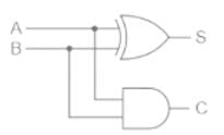
For the circuit shown, find the expression for 's'?- a)

- b)

- c)

- d)AB + A
Correct answer is option 'A'. Can you explain this answer?
For the circuit shown, find the expression for 's'?
a)
b)
c)
d)
AB + A
|
|
Pooja Patel answered |
Concept:
From the given figure:
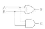
The above circuit is of Half adder:
- Sum (S) can be obtained by: A XOR B = A⨁ B
- Carry (C) can be obtained by: A AND B = A ∙ B
From the above truth table, it can conclude that:
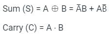
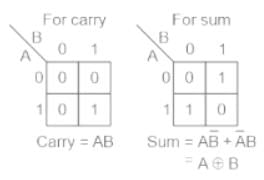
Fig: K-Map simplification of Half Adder
A 6 bit counter is used to count from 0, 1, 2, ......n. The value of n is _____- a)16
- b)15
- c)32
- d)63
Correct answer is option 'D'. Can you explain this answer?
A 6 bit counter is used to count from 0, 1, 2, ......n. The value of n is _____
a)
16
b)
15
c)
32
d)
63

|
Harshad Iyer answered |
Understanding a 6-Bit Counter
A 6-bit counter is a digital device that can store and count values using 6 binary digits (bits). Each bit can represent two states: 0 or 1.
Calculating the Maximum Count
- The maximum number of unique values a counter can represent is calculated using the formula:
2^n, where n is the number of bits.
- For a 6-bit counter:
2^6 = 64 unique values.
Counting Sequence
- A counter typically starts counting from 0, which means it will count from 0 to 63.
- Therefore, the values it can represent are:
0, 1, 2, ..., 63.
Determining the Value of n
- Since the counter starts at 0 and goes up to the maximum of 63, the highest value n that the counter can reach is:
n = 63.
Conclusion
- The correct answer to the question, "The value of n is _____" is:
Option D: 63.
This highlights the capability of a 6-bit counter to represent a range of values, emphasizing its utility in digital circuits and applications.
If two inputs are active on a priority encoder, which will be coded on the output?- a)The higher value
- b)The lower value
- c)Neither of the inputs
- d)Both of the inputs
Correct answer is option 'A'. Can you explain this answer?
If two inputs are active on a priority encoder, which will be coded on the output?
a)
The higher value
b)
The lower value
c)
Neither of the inputs
d)
Both of the inputs
|
|
Vaishnavi Nair answered |
Priority Encoding:
Priority encoding is a technique used in digital circuits to assign a unique code to the highest priority active input. It is commonly used in applications where multiple inputs need to be prioritized and encoded into a binary code.
Working Principle:
A priority encoder consists of multiple inputs and an output. The inputs are typically labeled as D0, D1, D2, etc., and the output provides a binary code corresponding to the highest priority active input. When multiple inputs are active simultaneously, the priority encoder assigns a code to the input with the highest priority.
Answer Explanation:
When two inputs are active on a priority encoder, the output will be coded based on the higher value input. This means that the input with the higher priority will be encoded on the output.
To understand this, let's consider a simple example of a 4-input priority encoder. The inputs are labeled as D0, D1, D2, and D3 (D0 being the highest priority). If both D2 and D3 are active, the output will be coded based on D3 because it has a higher priority than D2.
The priority encoder follows a priority order, where each input has a higher priority than the inputs below it. When multiple inputs are active, the priority encoder will prioritize the input with the highest priority and encode it on the output.
Example:
Let's consider a priority encoder with inputs D0, D1, and D2. The priority order is D0 > D1 > D2. If D1 and D2 are active simultaneously, the output will be coded based on D1 because it has a higher priority than D2. Similarly, if D0 and D2 are active simultaneously, the output will be coded based on D0.
In summary, when two inputs are active on a priority encoder, the input with the higher priority will be coded on the output. This ensures that the highest priority input is given precedence in the encoding process.
The size of encoder required for 4 bit flash type ADC is:- a)4 : 2
- b)4 : 1
- c)16 : 4
- d)16 : 1
Correct answer is option 'C'. Can you explain this answer?
The size of encoder required for 4 bit flash type ADC is:
a)
4 : 2
b)
4 : 1
c)
16 : 4
d)
16 : 1
|
|
Prasad Verma answered |
The size of the encoder required for a 4-bit flash-type ADC is 16:4.
Explanation:
Flash type ADC is a type of analog-to-digital converter that uses a combination of comparators to convert an analog input voltage into a digital output. In this type of ADC, the number of comparators used is equal to 2 raised to the power of the number of bits.
In a 4-bit flash ADC, we have 4 bits of resolution, which means we need 2^4 = 16 comparators. Each comparator compares the input voltage to a reference voltage and produces a high or low output depending on the comparison result.
To convert these 16 comparator outputs into a 4-bit digital output, we need an encoder. An encoder is a combinational logic circuit that converts the parallel output of the comparators into a serial digital output. The encoder maps the comparator outputs to the corresponding digital code.
In this case, we need to map the outputs of 16 comparators to a 4-bit digital output. Since we have 16 comparators, we need 16 input lines for the encoder. The number of output lines is equal to the number of bits in the digital output, which is 4 in this case.
So, the size of the encoder required for a 4-bit flash type ADC is 16:4, meaning 16 input lines and 4 output lines.
To summarize:
- Flash type ADC uses a combination of comparators to convert an analog input into a digital output.
- The number of comparators used in a flash ADC is equal to 2 raised to the power of the number of bits.
- In a 4-bit flash ADC, we need 16 comparators.
- An encoder is used to convert the parallel outputs of the comparators into a serial digital output.
- The size of the encoder required for a 4-bit flash ADC is 16:4, meaning 16 input lines and 4 output lines.
A sequence detector is designed to detect precisely 3 digital inputs, with overlapping sequences detectable. For the sequence (1,0,1) and input data (1,1,0,1,0,0,1,1,0,1,0,1,1,0), what is the output of this detector?- a)1,1,0,0,0,0,1,1,0,1,0,0
- b)0,1,0,0,0,0,0,1,0,1,0,0
- c)0,1,0,0,0,0,0,1,0,1,1,0
- d)0,1,0,0,0,0,0,0,1,0,0,0
Correct answer is option 'B'. Can you explain this answer?
A sequence detector is designed to detect precisely 3 digital inputs, with overlapping sequences detectable. For the sequence (1,0,1) and input data (1,1,0,1,0,0,1,1,0,1,0,1,1,0), what is the output of this detector?
a)
1,1,0,0,0,0,1,1,0,1,0,0
b)
0,1,0,0,0,0,0,1,0,1,0,0
c)
0,1,0,0,0,0,0,1,0,1,1,0
d)
0,1,0,0,0,0,0,0,1,0,0,0
|
|
Pooja Patel answered |
A sequence detector is a sequential circuit that outputs 1 when a particular pattern of bits sequentially arrives at its data input.
Given input data = 1,1,0,1,0,0,1,1,0,1,0,1,1,0
Overlapping sequences detectable.
The below table shows the output for each sequence:
The output = 0,1,0,0,0,0,0,1,0,1,0,0
The output = 0,1,0,0,0,0,0,1,0,1,0,0
Direction: Given question consists of two statements, one labeled as the 'Assertion (A)' and the other as 'Reason (R)'. You are to examine these two statements carefully and select the answers to these items using the codes given below.Assertion (A): A de-multiplexer cannot be used as a decoder.Reason (R): A de-multiplexer selects one of many outputs, whereas a decoder selects an output corresponding to the coded input.- a)Both A and R are individually true and R is the correct explanation of A
- b)Both A and R are individually true but R is NOT the correct explanation of A
- c)A is true but R is false
- d)A is false but R is true
Correct answer is option 'D'. Can you explain this answer?
Direction: Given question consists of two statements, one labeled as the 'Assertion (A)' and the other as 'Reason (R)'. You are to examine these two statements carefully and select the answers to these items using the codes given below.
Assertion (A): A de-multiplexer cannot be used as a decoder.
Reason (R): A de-multiplexer selects one of many outputs, whereas a decoder selects an output corresponding to the coded input.
a)
Both A and R are individually true and R is the correct explanation of A
b)
Both A and R are individually true but R is NOT the correct explanation of A
c)
A is true but R is false
d)
A is false but R is true

|
Naroj Boda answered |
Decoder:
Generally, a decoder converts a binary number into any other format (decimal, hexadecimal, etc)
Eg: 2 × 4 decoder
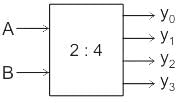
Truth Table:
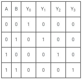
DeMUX: A demultiplexer takes a single input line and produces many output lines.
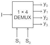
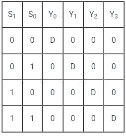
Now if we put input pin (I) of DeMUX remains at logic 1 and at select pin of DeMUX (S1, S0) we apply i / p (A, B) of decoder then DeMUX will be work as decoder. {I = 1}
Eg:
AB = 00 = S1 S0 ;
Y0 = 1 Y1 = 0 Y2 = 0 Y3 = 0
AB = 10 = S1 S0 ;
Y0 = 0 Y1 = 0 Y2 = 1 Y3 = 0
BCD to seven segment conversion is a ________________- a)Decoding process
- b)Encoding process
- c)Comparing process
- d)None of the mentioned
Correct answer is option 'A'. Can you explain this answer?
BCD to seven segment conversion is a ________________
a)
Decoding process
b)
Encoding process
c)
Comparing process
d)
None of the mentioned
|
|
Pooja Patel answered |
BCD to seven segment code conversion can be treated as a decoding process.
Half-adders have a major limitation in that they cannot __________- a)Accept a carry bit from a present stage
- b)Accept a carry bit from a next stage
- c)Accept a carry bit from a previous stage
- d)Accept a carry bit from the following stages
Correct answer is option 'C'. Can you explain this answer?
Half-adders have a major limitation in that they cannot __________
a)
Accept a carry bit from a present stage
b)
Accept a carry bit from a next stage
c)
Accept a carry bit from a previous stage
d)
Accept a carry bit from the following stages
|
|
Shanaya Mehta answered |
Limitation of Half-Adders
Half-adders are digital circuits that perform the addition of two binary digits. However, half-adders have a major limitation in that they cannot accept a carry bit from a previous stage. Let's understand this limitation in detail.
What is a Carry Bit?
A carry bit is generated when two binary digits are added together, and the result is greater than or equal to 2. In such a case, a carry bit is generated, which represents the carry-over to the next column of digits.
For example, when we add 1 + 1, the result is 10 in binary, where 1 is the sum and 0 is the carry bit.
Why Half-Adders Cannot Accept a Carry Bit from a Previous Stage?
Half-adders have two inputs, A and B, and two outputs, S (sum) and C (carry). The output S represents the sum of A and B, while the output C represents the carry-over to the next column of digits.
However, half-adders do not have any input to accept a carry bit from a previous stage. This means that if we want to add more than two binary digits, we need to use multiple half-adders connected in series, which is not an efficient way of performing addition.
For example, if we want to add three binary digits, A, B, and C, we need to use two half-adders. First, we add A and B using a half-adder to get the sum S1 and carry C1. Then, we add S1 and C using another half-adder to get the final sum S2 and carry C2.
However, if we had a full-adder instead of a half-adder, we could add three binary digits using only one full-adder, which is much more efficient.
Conclusion
In conclusion, half-adders have a major limitation in that they cannot accept a carry bit from a previous stage. This limitation makes it inefficient to perform addition of more than two binary digits using only half-adders. To overcome this limitation, we need to use full-adders or other advanced digital circuits.
Chapter doubts & questions for Combinational Logics - Analog and Digital Electronics 2025 is part of Electrical Engineering (EE) exam preparation. The chapters have been prepared according to the Electrical Engineering (EE) exam syllabus. The Chapter doubts & questions, notes, tests & MCQs are made for Electrical Engineering (EE) 2025 Exam. Find important definitions, questions, notes, meanings, examples, exercises, MCQs and online tests here.
Chapter doubts & questions of Combinational Logics - Analog and Digital Electronics in English & Hindi are available as part of Electrical Engineering (EE) exam.
Download more important topics, notes, lectures and mock test series for Electrical Engineering (EE) Exam by signing up for free.
Analog and Digital Electronics
135 videos|167 docs|71 tests
|
|
© EduRev
|
Education Revolution
|


|


Signup to see your scores
go up
within 7 days!
within 7 days!
Takes less than 10 seconds to signup