


All Exams >
Electrical Engineering (EE) >
Digital Electronics >
All Questions
All questions of Sequential Circuits for Electrical Engineering (EE) Exam
Assume that a 4-bit serial in/serial out shift register is initially clear. Bits are shifted in from left. We wish to store the nibble 1100. What will be the 4-bit pattern after the second clock pulse?- a)1100
- b)0011
- c)1111
- d)0000
Correct answer is option 'D'. Can you explain this answer?
Assume that a 4-bit serial in/serial out shift register is initially clear. Bits are shifted in from left. We wish to store the nibble 1100. What will be the 4-bit pattern after the second clock pulse?
a)
1100
b)
0011
c)
1111
d)
0000
|
|
Pooja Patel answered |
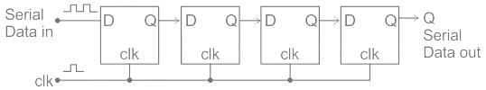
The register is given serial input with serial data 1100, the shift register is initially cleared 0000.
Since we have to store 1100 in the register, bits will be entered from the right.
The contents of the register after 1st pulse 0000.
Similarly, after the second shift, the contents of the register are 0000.
After the third clock pulse, the contents will be 1000
and after the fourth clock pulse, the contents will be 1100

A serial in/parallel out, 4-bit shift register initially contains all 1s. The data nibble 0111 is waiting to enter. After four clock pulses, the register contains ________- a)0000
- b)1111
- c)0111
- d)1000
Correct answer is option 'C'. Can you explain this answer?
A serial in/parallel out, 4-bit shift register initially contains all 1s. The data nibble 0111 is waiting to enter. After four clock pulses, the register contains ________
a)
0000
b)
1111
c)
0111
d)
1000

|
Pioneer Academy answered |
In Serial-In/Parallel-Out shift register, data will be shifted all at a time with every clock pulse. Therefore,
Wait | Store
0111 | 0000
011 | 1000 1st clk
01 | 1100 2nd clk
0 | 1110 3rd clk
X | 1111 4th clk.
Wait | Store
0111 | 0000
011 | 1000 1st clk
01 | 1100 2nd clk
0 | 1110 3rd clk
X | 1111 4th clk.
A ripple counter’s speed is limited by the propagation delay of ____________- a)Each flip-flop
- b)All flip-flops and gates
- c)The flip-flops only with gates
- d)Only circuit gates
Correct answer is option 'A'. Can you explain this answer?
A ripple counter’s speed is limited by the propagation delay of ____________
a)
Each flip-flop
b)
All flip-flops and gates
c)
The flip-flops only with gates
d)
Only circuit gates
|
|
Nishtha Chauhan answered |
A ripple counter is a type of digital counter circuit that uses flip-flops to sequentially count through a series of binary states. It is called a "ripple" counter because each flip-flop's output is connected to the clock input of the next flip-flop in the series, causing a ripple effect as each flip-flop changes state.
In a ripple counter, the first flip-flop is connected to an external clock signal, and each subsequent flip-flop is triggered by the output of the previous flip-flop. As the clock signal pulses, each flip-flop changes state and produces a binary output, which becomes the input for the next flip-flop. This sequential process creates a binary counting sequence.
The advantage of a ripple counter is its simplicity and low-cost design. However, it has a limitation in terms of speed, as the propagation delay from one flip-flop to the next accumulates with each stage, causing a time delay in the overall counting process.
Ripple counters are commonly used in applications where speed is not critical, such as simple digital displays, frequency dividers, or control circuits.
What happens to the parallel output word in an asynchronous binary down counter whenever a clock pulse occurs?- a)The output increases by 1
- b)The output decreases by 1
- c)The output word increases by 2
- d)The output word decreases by 2
Correct answer is option 'B'. Can you explain this answer?
What happens to the parallel output word in an asynchronous binary down counter whenever a clock pulse occurs?
a)
The output increases by 1
b)
The output decreases by 1
c)
The output word increases by 2
d)
The output word decreases by 2
|
|
Pooja Patel answered |
In an asynchronous counter, there isn’t any clock input. The output of 1st flip-flop is given to second flip-flop as clock input. So, in case of binary down counter the output word decreases by 1.
A J-K flip-flop can be obtained from the clocked S-R flip-flop by augmenting ___________- a)Two AND gates
- b)Two NAND gates
- c)Two NOT gates
- d)Two OR gates
Correct answer is option 'A'. Can you explain this answer?
A J-K flip-flop can be obtained from the clocked S-R flip-flop by augmenting ___________
a)
Two AND gates
b)
Two NAND gates
c)
Two NOT gates
d)
Two OR gates
|
|
Pooja Patel answered |
A J-K flip-flop can be obtained from the clocked S-R flip-flop by augmenting two AND gates.
A D flip-flop utilizing a PGT clock is in the CLEAR state. Which of the following input actions will cause it to change states?- a)CLK = NGT, D = 0
- b)CLK = PGT, D = 0
- c)CLOCK NGT, D = 1
- d)CLOCK PGT, D = 1
Correct answer is option 'D'. Can you explain this answer?
A D flip-flop utilizing a PGT clock is in the CLEAR state. Which of the following input actions will cause it to change states?
a)
CLK = NGT, D = 0
b)
CLK = PGT, D = 0
c)
CLOCK NGT, D = 1
d)
CLOCK PGT, D = 1
|
|
Pooja Patel answered |
PGT refers to Positive Going Transition and NGT refers to negative Going Transition. Earlier, the DFF is in a clear state (output is 0). So, if D = 1 then in the next stage output will be 1 and hence the stage will be changed.
A shift register that will accept a parallel input or a bidirectional serial load and internal shift features is called as?- a)Tristate
- b)End around
- c)Universal
- d)Conversion
Correct answer is option 'C'. Can you explain this answer?
A shift register that will accept a parallel input or a bidirectional serial load and internal shift features is called as?
a)
Tristate
b)
End around
c)
Universal
d)
Conversion
|
|
Pooja Patel answered |
A shift register can shift it’s data either left or right. The universal shift register is capable of shifting data left, right and parallel load capabilities.
Propagation delay of flip flops used for counter design largely affects the speed of operation of- a)asynchronous (ripple) counter
- b)synchronous up counter
- c)synchronous down counter
- d)synchronous up down counter
Correct answer is option 'A'. Can you explain this answer?
Propagation delay of flip flops used for counter design largely affects the speed of operation of
a)
asynchronous (ripple) counter
b)
synchronous up counter
c)
synchronous down counter
d)
synchronous up down counter
|
|
Kiran Iyer answered |
Propagation delay is the time it takes for a signal to propagate through a logic gate or flip flop. In the context of counter design, the propagation delay of flip flops plays a significant role in determining the speed of operation, especially in asynchronous (ripple) counters.
Asynchronous counters are designed using a series of flip flops, where the output of one flip flop serves as the clock input for the next flip flop in the chain. Each flip flop introduces a certain amount of propagation delay, which is the time it takes for the output of the flip flop to stabilize after a change in its inputs.
The main reason why the propagation delay of flip flops affects the speed of operation in asynchronous counters is due to the ripple effect. When the input to the first flip flop changes, it takes some time for the output of that flip flop to stabilize. This delay in stabilization propagates through the subsequent flip flops in the chain, causing a delay in the counting sequence.
The propagation delay can lead to several issues in asynchronous counters:
1. Skew: The propagation delay of flip flops can cause a skew in the counting sequence. Skew refers to the difference in arrival times of the clock signal at different flip flops. This can result in an inconsistent and unpredictable counting sequence.
2. Glitches: The propagation delay can also cause glitches in the counter output. A glitch is a temporary and unwanted change in the output of a logic circuit. Due to the ripple effect, glitches can occur when the outputs of the flip flops are changing during the stabilization period.
3. Limited frequency of operation: Asynchronous counters have a limited operating frequency due to the cumulative effect of propagation delays. If the input clock signal has a high frequency, the propagation delays can accumulate and result in errors or unpredictable behavior in the counter.
On the other hand, synchronous counters, both up and down, do not suffer from these issues because they use a common clock signal to synchronize all flip flops simultaneously. The propagation delay of individual flip flops still exists but does not affect the counting sequence or introduce glitches, as all flip flops are updated at the same time.
In conclusion, the propagation delay of flip flops largely affects the speed of operation in asynchronous (ripple) counters due to the ripple effect, which can lead to skew, glitches, and limitations on the operating frequency.
The register is a type of ___________- a)Sequential circuit
- b)Combinational circuit
- c)CPU
- d)Latches
Correct answer is option 'A'. Can you explain this answer?
The register is a type of ___________
a)
Sequential circuit
b)
Combinational circuit
c)
CPU
d)
Latches
|
|
Pooja Patel answered |
Register’s output depends on the past and present states of the inputs. The device which follows these properties is termed as a sequential circuit. Whereas, combinational circuits only depend on the present values of inputs.
A basic S-R flip-flop can be constructed by cross-coupling of which basic logic gates?- a)AND or OR gates
- b)XOR or XNOR gates
- c)NOR or NAND gates
- d)AND or NOR gates
Correct answer is option 'C'. Can you explain this answer?
A basic S-R flip-flop can be constructed by cross-coupling of which basic logic gates?
a)
AND or OR gates
b)
XOR or XNOR gates
c)
NOR or NAND gates
d)
AND or NOR gates
|
|
Sushant Mehta answered |
Basic S-R Flip-Flop
The basic S-R (Set-Reset) flip-flop is a type of sequential logic circuit that can store one bit of information. It is constructed by cross-coupling two NOR (Negative-OR) gates.
Cross-Coupling of NOR Gates
To understand why the cross-coupling of NOR gates is used to construct an S-R flip-flop, let's first examine the truth table of a NOR gate:
Set and Reset Inputs
In an S-R flip-flop, the two inputs are called the Set and Reset inputs. When the Set input is high (1), it sets the flip-flop to the high (1) state. Conversely, when the Reset input is high (1), it resets the flip-flop to the low (0) state.
Construction of S-R Flip-Flop
To construct an S-R flip-flop using NOR gates, we connect the output of one NOR gate to the Set input of the other NOR gate, and vice versa. This creates a feedback loop between the two gates, allowing the flip-flop to store information.
Working Principle
1. Initially, both inputs are low (0), and the outputs of both NOR gates are high (1).
2. When the Set input is activated (high), the output of the first NOR gate goes low (0), which is fed back to the Set input of the second NOR gate. This causes the output of the second NOR gate to go high (1), setting the flip-flop to the high state.
3. If the Set input returns to low (0), the flip-flop remains in the high state.
4. Similarly, when the Reset input is activated (high), the output of the second NOR gate goes low (0), which is fed back to the Reset input of the first NOR gate. This causes the output of the first NOR gate to go high (1), resetting the flip-flop to the low state.
5. If the Reset input returns to low (0), the flip-flop remains in the low state.
Summary
In summary, the cross-coupling of NOR gates allows the construction of a basic S-R flip-flop. The Set and Reset inputs control the state of the flip-flop, and the feedback loop between the gates maintains the stored information. This flip-flop is a fundamental building block in digital systems, and its behavior can be further modified and enhanced using additional logic gates.
The basic S-R (Set-Reset) flip-flop is a type of sequential logic circuit that can store one bit of information. It is constructed by cross-coupling two NOR (Negative-OR) gates.
Cross-Coupling of NOR Gates
To understand why the cross-coupling of NOR gates is used to construct an S-R flip-flop, let's first examine the truth table of a NOR gate:
| A | B | Output |
|---|---|---|
| 0 | 0 | 1 |
| 0 | 1 | 0 |
| 1 | 0 | 0 |
| 1 | 1 | 0 |
Set and Reset Inputs
In an S-R flip-flop, the two inputs are called the Set and Reset inputs. When the Set input is high (1), it sets the flip-flop to the high (1) state. Conversely, when the Reset input is high (1), it resets the flip-flop to the low (0) state.
Construction of S-R Flip-Flop
To construct an S-R flip-flop using NOR gates, we connect the output of one NOR gate to the Set input of the other NOR gate, and vice versa. This creates a feedback loop between the two gates, allowing the flip-flop to store information.
Working Principle
1. Initially, both inputs are low (0), and the outputs of both NOR gates are high (1).
2. When the Set input is activated (high), the output of the first NOR gate goes low (0), which is fed back to the Set input of the second NOR gate. This causes the output of the second NOR gate to go high (1), setting the flip-flop to the high state.
3. If the Set input returns to low (0), the flip-flop remains in the high state.
4. Similarly, when the Reset input is activated (high), the output of the second NOR gate goes low (0), which is fed back to the Reset input of the first NOR gate. This causes the output of the first NOR gate to go high (1), resetting the flip-flop to the low state.
5. If the Reset input returns to low (0), the flip-flop remains in the low state.
Summary
In summary, the cross-coupling of NOR gates allows the construction of a basic S-R flip-flop. The Set and Reset inputs control the state of the flip-flop, and the feedback loop between the gates maintains the stored information. This flip-flop is a fundamental building block in digital systems, and its behavior can be further modified and enhanced using additional logic gates.
How many flip-flops are required to build a binary counter circuit to count from 0 to 1023 ?- a)1
- b)6
- c)10
- d)23
Correct answer is option 'C'. Can you explain this answer?
How many flip-flops are required to build a binary counter circuit to count from 0 to 1023 ?
a)
1
b)
6
c)
10
d)
23
|
|
Pooja Patel answered |
Concept:
Counters:
- It is a sequential logic circuit that has a clock input signal and a group of output signals
- It represents an integer "counts" value.
- Internally, counters use flip-flops to represent the current counts and to retain the counts between clocks.
- N values can be counted with n number of flip flops. its relation is given by-
2n ≥ N
where, N = number of counts
n = number of flip flops
Calculation-
Given- N= 1023
2n ≥ 1023
n = 10
Hence total of 10 flip flops are required to count from 0 to 1023.
The truth table for an S-R flip-flop has how many VALID entries?- a)1
- b)2
- c)3
- d)4
Correct answer is option 'C'. Can you explain this answer?
The truth table for an S-R flip-flop has how many VALID entries?
a)
1
b)
2
c)
3
d)
4
|
|
Pooja Patel answered |
The SR flip-flop actually has three inputs, Set, Reset and its current state. The Invalid or Undefined State occurs at both S and R being at 1.
How many types of triggering take place in a flip flops?- a)3
- b)2
- c)4
- d)5
Correct answer is option 'A'. Can you explain this answer?
How many types of triggering take place in a flip flops?
a)
3
b)
2
c)
4
d)
5
|
|
Pooja Patel answered |
There are three types of triggering in a flip-flop, viz., level triggering, edge triggering and pulse triggering.
If the input to T-flipflop is 200 Hz signal, the final output of the three T- flipflops in cascade is- a)25 Hz
- b)20 Hz
- c)50 Hz
- d)12.5 Hz
Correct answer is option 'A'. Can you explain this answer?
If the input to T-flipflop is 200 Hz signal, the final output of the three T- flipflops in cascade is
a)
25 Hz
b)
20 Hz
c)
50 Hz
d)
12.5 Hz
|
|
Mahesh Singh answered |
Explanation:
The T-flipflop is a type of flipflop that toggles its output based on the input signal. It has two inputs: T (toggle) and CLK (clock) and one output Q.
Given:
Input signal frequency = 200 Hz
Working:
When a T-flipflop receives a pulse at its CLK input, it toggles its output (Q) based on the value of the T input. If T = 0, the output remains the same, and if T = 1, the output flips.
In a cascade connection of three T-flipflops, the output of one flipflop is connected to the CLK input of the next flipflop. This means that the output of the first flipflop becomes the input to the second flipflop, and so on.
Since the input signal to the first T-flipflop is a 200 Hz signal, the output of this flipflop will toggle at 200 Hz. This means that the output will change its state (from 0 to 1 or from 1 to 0) 200 times per second.
Now, the output of the first flipflop becomes the input to the second flipflop. Since the output of the first flipflop toggles at 200 Hz, the input to the second flipflop will also toggle at the same frequency.
Similarly, the output of the second flipflop becomes the input to the third flipflop. So, the input to the third flipflop will also toggle at 200 Hz.
Therefore, the final output of the three T-flipflops in cascade will also toggle at 200 Hz.
Conclusion:
The final output of the three T-flipflops in cascade is 200 Hz.
Therefore, the correct answer is option 'A' (25 Hz).
The terminal count of a typical modulus-10 binary counter is ____________- a)0000
- b)1010
- c)1001
- d)1111
Correct answer is option 'C'. Can you explain this answer?
The terminal count of a typical modulus-10 binary counter is ____________
a)
0000
b)
1010
c)
1001
d)
1111
|
|
Pooja Patel answered |
A binary counter counts or produces the equivalent binary number depending on the cycles of the clock input. Modulus-10 means count from 0 to 9. So, the terminal count is 9 (1001).
D flip-flop is a circuit having ____________- a)2 NAND gates
- b)3 NAND gates
- c)4 NAND gates
- d)5 NAND gates
Correct answer is option 'C'. Can you explain this answer?
D flip-flop is a circuit having ____________
a)
2 NAND gates
b)
3 NAND gates
c)
4 NAND gates
d)
5 NAND gates
|
|
Pooja Patel answered |
D flip-flop is a circuit having 4 NAND gates. Two of them are connected with each other.
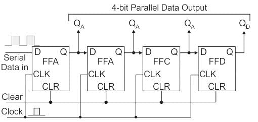
What is the mod number of asynchronous counter shown (All J = K = 1) below: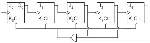
- a)24
- b)48
- c)29
- d)28
Correct answer is option 'D'. Can you explain this answer?
What is the mod number of asynchronous counter shown (All J = K = 1) below:
a)
24
b)
48
c)
29
d)
28
|
|
Pioneer Academy answered |
Concept:
Counters are characterized by the clock connection & triggering of the clock, as explained below:
Analysis:
- In the given circuit, each of the JK flip-flops is negative edge triggered & the clock connection is with ‘Q’. So it is an up counter.
- The output of each flip-flop will be cleared i.e 0 Only when the output from the NAND gate is '0'. So, to get we have to obtain the outputs from flip-flops 2nd,3rd & 4rth as '1' i.e Q4, Q3, Q2 = 1
- So when Q4, Q3 & Q2 simultaneously are equal to 1 for the first time, the counter will reset.
So, the sequence of counter states for consecutive clock pulses are as follows:
Here Q4, Q3 & Q2 will be ‘1’ simultaneously for the first time after 28th Clock Pulse is what we observe.
So the given counter is a mode-28 up counter because it can show up in only 28 states.
A basic S-R flip-flop can be constructed by cross-coupling of which basic logic gates?- a)AND or OR gates
- b)XOR or XNOR gates
- c)NOR or NAND gates
- d)AND or NOR gates
Correct answer is option 'C'. Can you explain this answer?
A basic S-R flip-flop can be constructed by cross-coupling of which basic logic gates?
a)
AND or OR gates
b)
XOR or XNOR gates
c)
NOR or NAND gates
d)
AND or NOR gates
|
|
Pallavi Nair answered |
S-R Flip-Flop Construction using NOR gates
To construct a basic S-R flip-flop, we can use a combination of NOR gates. The S-R flip-flop is a fundamental building block in digital circuits and is used to store a single bit of information. It has two inputs, S (set) and R (reset), and two outputs, Q and Q̅ (complement of Q).
Truth Table
The truth table of an S-R flip-flop is as follows:
S | R | Q | Q̅
--|---|---|---
0 | 0 | Q | Q̅
0 | 1 | 0 | 1
1 | 0 | 1 | 0
1 | 1 | - | -
Design using NOR gates
The cross-coupling of NOR gates allows us to implement an S-R flip-flop. Here is the construction using NOR gates:
1. Connect the S input to one input of a NOR gate and the R input to one input of another NOR gate.
2. Connect the Q output to one input of the NOR gate corresponding to the R input.
3. Connect the Q̅ output to one input of the NOR gate corresponding to the S input.
4. Connect the output of the NOR gate connected to the R input to the other input of the NOR gate connected to the S input.
5. Connect the output of the NOR gate connected to the S input to the other input of the NOR gate connected to the R input.
Explanation
When both S and R inputs are low (0), the NOR gates produce high outputs, maintaining the previous state of the flip-flop. This forms a stable state where Q and Q̅ remain unchanged.
When S is high (1) and R is low (0), the NOR gate connected to S input produces a low output, which is connected to the R input NOR gate. This results in a high output at Q and a low output at Q̅, setting the flip-flop to the state Q=1.
Similarly, when S is low (0) and R is high (1), the NOR gate connected to R input produces a low output, which is connected to the S input NOR gate. This results in a low output at Q and a high output at Q̅, resetting the flip-flop to the state Q=0.
Finally, when both S and R inputs are high (1), it creates a condition called the "forbidden" state, where the outputs of the NOR gates are unpredictable. Therefore, this state is avoided in practical designs.
Thus, the cross-coupling of NOR gates allows us to construct a basic S-R flip-flop that can store and manipulate a single bit of information.
Consider the circuit shown below: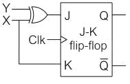 The characteristic equation of the new flip-flop created from the above circuit is
- a)Y̅ (X̅ + Qn) + XY̅Q̅n
- b)X̅ (Y + Qn) + XY̅Q̅n
- c)Qn (Y + X̅) + X̅YQ̅n
- d)Qn (Y̅ + X̅) + XYQn
Correct answer is option 'B'. Can you explain this answer?
Consider the circuit shown below:
The characteristic equation of the new flip-flop created from the above circuit is
a)
Y̅ (X̅ + Qn) + XY̅Q̅n
b)
X̅ (Y + Qn) + XY̅Q̅n
c)
Qn (Y + X̅) + X̅YQ̅n
d)
Qn (Y̅ + X̅) + XYQn
|
|
Pioneer Academy answered |
For J-K flip-flop,
Qn+1 = JQ̅n + K̅Qn ----(1)

For the given circuit:
J = X ⊕ Y and K = X
From equation (1);
Qn+1 = (X ⊕ Y)Q̅n + X̅Qn
= X̅YQ̅n + X̅Qn + XY̅Q̅n
= X̅Qn + X̅YQ̅n + XY̅Q̅n
= X̅ (YQ̅n + Qn) + XY̅Q̅n
= X̅ (Y + Qn) + XY̅Q̅n
Hence, option 2 is correct.
How many natural states will there be in a 4-bit ripple counter?- a)4
- b)8
- c)16
- d)32
Correct answer is option 'C'. Can you explain this answer?
How many natural states will there be in a 4-bit ripple counter?
a)
4
b)
8
c)
16
d)
32
|
|
Samarth Khanna answered |
The number of natural states in a 4-bit ripple counter can be determined by considering the number of possible combinations of its 4 bits.
- Decimal System:
In the decimal system, we have 10 digits (0-9) to represent numbers. Similarly, in a binary system, we have 2 digits (0 and 1) to represent numbers.
- Binary Number Representation:
A 4-bit ripple counter has 4 bits, which means it can represent 2^4 = 16 different states. Each bit can be either 0 or 1, so the total number of possible combinations is 2^4 = 16.
- Counting the States:
To understand the counting of states, let's consider a simple example of a 3-bit ripple counter. In a 3-bit counter, we have 3 bits that can be either 0 or 1.
- Number of States:
The number of states can be calculated using the formula 2^n, where n is the number of bits. In the case of a 3-bit counter, the number of states is 2^3 = 8. Similarly, in a 4-bit counter, the number of states is 2^4 = 16.
- Explanation:
In a ripple counter, the output of one flip-flop serves as the clock input to the next flip-flop. Each flip-flop represents one bit, and the number of bits determines the number of possible states.
- Each Bit:
Each bit can independently toggle between 0 and 1. So, for a 4-bit counter, each bit has 2 possible states (0 or 1).
- Total States:
To calculate the total number of states, we multiply the number of states for each bit. In this case, since we have 4 bits, the total number of states is 2 * 2 * 2 * 2 = 16.
Therefore, the correct answer is option 'C' - 16.
What is the time delay (td) of an 8-bit serial in/serial out shift register with a clock frequency of 4 MHz?- a)0.2 μs
- b)8 μs
- c)4 μs
- d)2 μs
Correct answer is option 'D'. Can you explain this answer?
What is the time delay (td) of an 8-bit serial in/serial out shift register with a clock frequency of 4 MHz?
a)
0.2 μs
b)
8 μs
c)
4 μs
d)
2 μs
|
|
Prerna Tiwari answered |
Ms
To calculate the time delay (td) of an 8-bit serial in/serial out shift register, we need to consider the number of bits being shifted and the clock frequency.
The time delay can be calculated using the formula:
td = (Number of bits x Clock cycle time)
Given that we have an 8-bit register and a clock frequency of 4 MHz (4 x 10^6 Hz), we can calculate the time delay as follows:
td = (8 bits x 1/(4 x 10^6 Hz)) = 8 x 0.25 microseconds = 2 microseconds
Therefore, the time delay (td) of an 8-bit serial in/serial out shift register with a clock frequency of 4 MHz is 2 microseconds.
Internal propagation delay of asynchronous counter is removed by ____________- a)Ripple counter
- b)Ring counter
- c)Modulus counter
- d)Synchronous counter
Correct answer is option 'D'. Can you explain this answer?
Internal propagation delay of asynchronous counter is removed by ____________
a)
Ripple counter
b)
Ring counter
c)
Modulus counter
d)
Synchronous counter
|
|
Bijoy Mehta answered |
Internal Propagation Delay of Asynchronous Counter
The internal propagation delay of an asynchronous counter refers to the time delay between the input signal and the output signal of each flip-flop within the counter. Asynchronous counters are also known as ripple counters because the output of each flip-flop ripples through to the next flip-flop, causing a delay in the output signal.
Synchronous Counter
A synchronous counter, on the other hand, is a type of counter where all the flip-flops within the counter are clocked simultaneously by a common clock signal. This means that the output of each flip-flop is updated at the same time, eliminating the propagation delay between the flip-flops.
Elimination of Internal Propagation Delay
The internal propagation delay of an asynchronous counter can cause timing issues and glitches in the output signal, especially at higher frequencies. To overcome this issue, a synchronous counter is used. When all the flip-flops within the counter are clocked simultaneously, the internal propagation delay is eliminated.
Advantages of Synchronous Counter
- Elimination of Propagation Delay: The synchronous counter ensures that the output of each flip-flop is updated at the same time, eliminating the delay between the flip-flops. This results in a more accurate and synchronized output signal.
- Improved Timing: Synchronous counters offer better timing characteristics compared to asynchronous counters. The synchronous operation allows for precise control of the clock signal, ensuring accurate counting and timing.
- Higher Speed Operation: Due to the elimination of the propagation delay, synchronous counters can operate at higher clock frequencies without the risk of glitches or timing errors.
- Better Design Flexibility: Synchronous counters are easier to design and analyze because the timing characteristics are more predictable. This allows for more complex counter configurations and applications.
Conclusion
The internal propagation delay of an asynchronous counter is removed by using a synchronous counter. The synchronous operation ensures that all flip-flops within the counter are clocked simultaneously, eliminating the delay between the flip-flops and improving the overall timing and accuracy of the counter.
When both inputs of SR latches are low, the latch ___________- a)Q output goes high
- b)Q’ output goes high
- c)It remains in its previously set or reset state
- d)it goes to its next set or reset state
Correct answer is option 'C'. Can you explain this answer?
When both inputs of SR latches are low, the latch ___________
a)
Q output goes high
b)
Q’ output goes high
c)
It remains in its previously set or reset state
d)
it goes to its next set or reset state
|
|
Prateek Mehra answered |
Output goes lowc)Q output remains unchangedd)Q output toggles between high and low
For which of the following flip-flops, the output is clearly defined for all combinations of two inputs.- a)D type flip-flop
- b)R-S flip-flop
- c)J-K flip-flop
- d)T flip-flop
Correct answer is option 'C'. Can you explain this answer?
For which of the following flip-flops, the output is clearly defined for all combinations of two inputs.
a)
D type flip-flop
b)
R-S flip-flop
c)
J-K flip-flop
d)
T flip-flop
|
|
Pooja Patel answered |
For R-S flip-flop for input 1,1 the output is undefined.
The truth table of J-K -flop-flop is
The output is clearly defined for all combinations of inputs.
Both D type and T type flip-flops have only one input.
The S-R, J-K and D inputs are called ____________- a)Asynchronous inputs
- b)Synchronous inputs
- c)Bidirectional inputs
- d)Unidirectional inputs
Correct answer is option 'B'. Can you explain this answer?
The S-R, J-K and D inputs are called ____________
a)
Asynchronous inputs
b)
Synchronous inputs
c)
Bidirectional inputs
d)
Unidirectional inputs
|
|
Pooja Patel answered |
The S-R, J-K and D inputs are called synchronous inputs because data on these inputs are transferred to the flip-flop’s output only on the triggering edge or level triggering of the clock pulse. Moreover, flip-flops have a clock input whereas latches don’t. Hence, known as synchronous inputs.
Master slave flip flop is also referred to as?- a)Level triggered flip flop
- b)Pulse triggered flip flop
- c)Edge triggered flip flop
- d)Edge-Level triggered flip flop
Correct answer is option 'B'. Can you explain this answer?
Master slave flip flop is also referred to as?
a)
Level triggered flip flop
b)
Pulse triggered flip flop
c)
Edge triggered flip flop
d)
Edge-Level triggered flip flop
|
|
Pallabi Pillai answered |
Master-slave flip flop is a type of sequential logic circuit that can store one bit of binary information. It is commonly used in digital electronics for various applications such as memory elements, counters, and registers. This type of flip flop is also referred to as a pulse-triggered flip flop because it changes its output state in response to a specific pulse.
The master-slave flip flop consists of two D flip flops, namely the master and the slave flip flops. These two flip flops are connected in series, with the output of the master flip flop connected to the input of the slave flip flop.
The operation of the master-slave flip flop can be divided into two phases: the master phase and the slave phase.
Master Phase:
During the master phase, the master flip flop is enabled, and the input signal is allowed to propagate through the circuit. The input signal is applied to the master flip flop, and its state is stored. However, the output of the master flip flop is not directly connected to the output of the circuit.
Slave Phase:
During the slave phase, the master flip flop is disabled, and the slave flip flop is enabled. The stored state of the master flip flop is transferred to the slave flip flop, which then becomes the output of the circuit. This transfer of data occurs when a clock pulse triggers the transition from the master phase to the slave phase.
The clock pulse acts as a trigger for the master-slave flip flop. It synchronizes the operation of the flip flop and ensures that the state transfer occurs at the appropriate time.
In summary, the master-slave flip flop is referred to as a pulse-triggered flip flop because it changes its output state in response to a clock pulse. This type of flip flop is widely used in digital electronics due to its reliable and synchronized operation.
In S-R latch, when the SET input is made high, output Q becomes:- a)0
- b)1
- c)no change
- d)application not allowed
Correct answer is option 'B'. Can you explain this answer?
In S-R latch, when the SET input is made high, output Q becomes:
a)
0
b)
1
c)
no change
d)
application not allowed
|
|
Naveen Kapoor answered |
Effect of SET input in S-R latch:
When the SET input of an S-R latch is made high, it sets the latch, causing the Q output to become high.
Explanation:
- When the SET input is activated, it overrides the RESET input and forces the Q output to be high.
- This behavior is due to the internal logic of the S-R latch, where the SET input triggers the latch to store a high output.
- The Q output will remain high until a reset signal is applied to the latch.
Conclusion:
In summary, when the SET input of an S-R latch is made high, the output Q will be set to a high state, which can be represented as logic level 1.
Three T flip flops are connected to form a counter. The maximum states possible for the counter will be:- a)5
- b)3
- c)8
- d)7
Correct answer is option 'C'. Can you explain this answer?
Three T flip flops are connected to form a counter. The maximum states possible for the counter will be:
a)
5
b)
3
c)
8
d)
7
|
|
Bijoy Mehta answered |
The correct answer is option 'C', 8 states.
Explanation:
To understand why the maximum states possible for the counter formed by three T flip-flops is 8, we need to understand the operation of a T flip-flop and how it can be used to build a counter.
1. T Flip-Flop:
A T flip-flop is a type of flip-flop that toggles its output based on the input signal. It has a single input (T) and a single output (Q). The output changes state (toggles) when the input is high (1) and remains the same when the input is low (0).
2. Counter Operation:
A counter is a digital circuit that counts the number of events or occurrences of a specific signal. In this case, we are using three T flip-flops to build a counter.
- Initially, all the flip-flops are reset to 0.
- When a clock pulse is applied, the first flip-flop (FF1) toggles its output.
- The output of FF1 is connected to the input of the second flip-flop (FF2).
- When the next clock pulse is applied, FF2 toggles its output based on the input from FF1.
- The output of FF2 is connected to the input of the third flip-flop (FF3).
- When the next clock pulse is applied, FF3 toggles its output based on the input from FF2.
3. Maximum States:
To determine the maximum states possible for the counter, we need to consider the number of unique combinations of outputs from the three flip-flops.
- Each flip-flop has two possible output states: 0 or 1.
- For three flip-flops, the total number of possible combinations is 2^3 = 8.
Therefore, the maximum states possible for the counter formed by three T flip-flops will be 8 (option 'C'). These states can be represented by the binary numbers from 000 to 111.
When both the inputs of a latch are high, the output is unpredictable. What is this condition called?- a)Bistable
- b)Indeterminate
- c)Inactive
- d)No change
Correct answer is option 'B'. Can you explain this answer?
When both the inputs of a latch are high, the output is unpredictable. What is this condition called?
a)
Bistable
b)
Indeterminate
c)
Inactive
d)
No change
|
|
Anirban Gupta answered |
Indeterminate Output Condition in a Latch
Explanation:
When both inputs of a latch are high, meaning that both inputs are at logic level 1, the output of the latch becomes unpredictable. This condition is known as the indeterminate output condition.
Reason for Indeterminate Output:
The indeterminate output condition occurs because both inputs being high causes the latch to enter a metastable state. In this state, the outputs oscillate rapidly between logic 0 and logic 1, resulting in an unpredictable output.
Metastability:
Metastability is a phenomenon that occurs in digital circuits when a flip-flop or latch is in a state of uncertainty or oscillation between logic levels. It can happen when the inputs to the flip-flop or latch change close to the edge of a clock signal. Metastability can cause the output to remain in an unknown state for an indefinite period of time until it eventually stabilizes.
Consequences of Indeterminate Output:
The indeterminate output condition can have several consequences:
1. Data corruption: The unpredictable output can lead to errors in the data being processed or stored by the latch.
2. Timing issues: The indeterminate output can affect the timing of subsequent logic operations, causing timing violations and potential malfunctioning of the circuit.
3. System instability: The unpredictable output can propagate through the system, leading to unstable behavior and unreliable operation.
Preventing Indeterminate Output:
To prevent the indeterminate output condition in a latch, it is important to ensure that both inputs are not simultaneously high. This can be achieved by using proper timing and sequencing of input signals. It is also common practice to use edge-triggered flip-flops instead of latches in critical circuits, as flip-flops have built-in synchronization mechanisms to avoid metastability issues.
Conclusion:
The indeterminate output condition occurs in a latch when both inputs are high, causing the latch to enter a metastable state. This condition can lead to unpredictable outputs, data corruption, timing issues, and system instability. It is important to prevent this condition by carefully designing the timing and sequencing of input signals and considering the use of edge-triggered flip-flops instead of latches in critical circuits.
The main difference between a register and a counter is ___________- a)A register has no specific sequence of states
- b)A counter has no specific sequence of states
- c)A register has capability to store one bit of information but counter has n-bit
- d)A register counts data
Correct answer is option 'A'. Can you explain this answer?
The main difference between a register and a counter is ___________
a)
A register has no specific sequence of states
b)
A counter has no specific sequence of states
c)
A register has capability to store one bit of information but counter has n-bit
d)
A register counts data
|
|
Pooja Patel answered |
The main difference between a register and a counter is that a register has no specific sequence of states except in certain specialised applications.
The circuits of NOR based S-R latch classified as asynchronous sequential circuits, why?- a)Because of inverted outputs
- b)Because of triggering functionality
- c)Because of cross-coupled connection
- d)Because of inverted outputs & triggering functionality
Correct answer is option 'C'. Can you explain this answer?
The circuits of NOR based S-R latch classified as asynchronous sequential circuits, why?
a)
Because of inverted outputs
b)
Because of triggering functionality
c)
Because of cross-coupled connection
d)
Because of inverted outputs & triggering functionality
|
|
Ameya Gupta answered |
C) Because of cross-coupled connection
The circuits of NOR based S-R latch are classified as asynchronous sequential circuits primarily because of their cross-coupled connection. In a NOR based S-R latch, the output of one NOR gate is connected to the input of the other NOR gate, creating a feedback loop. This cross-coupling allows the latch to store a state or hold information, making it a sequential circuit.
The inverted outputs (d) and triggering functionality (b) are also characteristics of NOR based S-R latch but are not the main reasons for classifying it as an asynchronous sequential circuit.
One example of the use of an S-R flip-flop is as ___________- a)Transition pulse generator
- b)Racer
- c)Switch debouncer
- d)Astable oscillator
Correct answer is option 'C'. Can you explain this answer?
One example of the use of an S-R flip-flop is as ___________
a)
Transition pulse generator
b)
Racer
c)
Switch debouncer
d)
Astable oscillator
|
|
Sparsh Nambiar answered |
S-R Flip-Flop as a Switch Debouncer
Switch debouncing is a process used to eliminate the noise or chatter caused by mechanical switches when they are being pressed or released. This noise can result in multiple false transitions, which can interfere with the proper functioning of digital circuits. One way to debounce a switch is by using an S-R flip-flop.
What is an S-R Flip-Flop?
A flip-flop is a sequential logic circuit that can store one bit of information. The S-R (Set-Reset) flip-flop is one of the most widely used types of flip-flops. It has two inputs, S (set) and R (reset), and two outputs, Q (output) and Q' (complement of the output).
Operation of an S-R Flip-Flop
- When the S input is HIGH and the R input is LOW, the flip-flop is set, and the Q output goes HIGH.
- When the R input is HIGH and the S input is LOW, the flip-flop is reset, and the Q output goes LOW.
- When both inputs are HIGH, the flip-flop is in an indeterminate state, which is not desirable for proper operation.
Switch Debouncing with an S-R Flip-Flop
To use an S-R flip-flop as a switch debouncer, the switch is connected to the S input, and its complement (inverse) is connected to the R input. The Q output of the flip-flop is then connected to the input of the digital circuit.
When the switch is pressed or released, it may generate multiple transitions due to mechanical bouncing. These transitions may cause the digital circuit to behave unexpectedly. However, the S-R flip-flop eliminates these unwanted transitions by ensuring that the Q output stabilizes at the final desired state.
Working Principle
- Initially, both the S and R inputs of the flip-flop are LOW.
- When the switch is pressed, the S input goes HIGH, causing the flip-flop to set and the Q output to go HIGH.
- As long as the switch remains pressed, the S input remains HIGH, but the flip-flop does not change its state due to the stable latch behavior.
- When the switch is released, the S input goes LOW, but the flip-flop maintains its state, and the Q output remains HIGH.
- Similarly, when the switch is pressed again, the R input goes HIGH, causing the flip-flop to reset and the Q output to go LOW.
- As long as the switch remains pressed, the R input remains HIGH, but the flip-flop does not change its state.
- When the switch is released again, the R input goes LOW, but the flip-flop maintains its state, and the Q output remains LOW.
Advantages of Using an S-R Flip-Flop for Switch Debouncing
- Simple and cost-effective solution for eliminating switch noise.
- Provides a stable output state unaffected by switch bouncing.
- Can be easily implemented using basic logic gates.
- Suitable for both manual and mechanical switches.
Conclusion
Using an S-R flip-flop as a switch debouncer is an effective way to remove noise and ensure the proper functioning of digital circuits. By connecting the switch to the S input and its complement to the R input, the flip-flop provides a stable output state
The output Qn of a JK flip-flop is zero. It changes to 1 when a clock pulse is applied. The input Jn and Kn are respectively- a)1 and X
- b)0 and X
- c)X and 0
- d)X and 1
Correct answer is option 'A'. Can you explain this answer?
The output Qn of a JK flip-flop is zero. It changes to 1 when a clock pulse is applied. The input Jn and Kn are respectively
a)
1 and X
b)
0 and X
c)
X and 0
d)
X and 1
|
|
Ashwin Kapoor answered |
Explanation:
To understand the given question and the correct answer, let's first review the operation of a JK flip-flop.
A JK flip-flop is a sequential logic device that has two inputs, J (set) and K (reset), and two outputs, Q (output) and Q' (complement of the output). The flip-flop operates based on clock pulses, which determine when the inputs are accepted and when the outputs are updated.
The behavior of a JK flip-flop is defined by its truth table:
Truth Table:
J K Qn Qn+1
0 0 0 0
0 0 1 1
0 1 0 0
0 1 1 0
1 0 0 1
1 0 1 1
1 1 0 1
1 1 1 0
In the given question, it is stated that the output Q of the JK flip-flop is initially 0. When a clock pulse is applied, the output changes to 1. Based on this information, we can deduce the values of the J and K inputs.
Analysis:
Since the initial output Q is 0 and changes to 1 on a clock pulse, we need to find the input combination that satisfies this behavior.
From the truth table, we observe that the output Q changes to 1 when J is 1 and K is 0. This is the only input combination that results in a change from 0 to 1 on the output Q.
Therefore, the correct answer is option 'A' - J = 1 and K = X (don't care).
Explanation:
The reason why the correct answer is J = 1 and K = X (don't care) can be explained as follows:
When J = 1 and K = X (don't care), the flip-flop operates in the following manner:
- When the clock pulse is applied, the flip-flop checks the values of J and K.
- Since J is 1, the flip-flop sets the output Q to 1, regardless of the value of K.
- As a result, the output Q changes from 0 to 1 on the clock pulse.
It is important to note that in this specific scenario, the value of K is not relevant because the J input takes precedence. When J is 1, the output Q will always change to 1, regardless of the value of K.
This behavior is specific to the JK flip-flop and is not applicable to other types of flip-flops, such as D or T flip-flops.
Conclusion:
In summary, the output Q of a JK flip-flop changes from 0 to 1 when a clock pulse is applied. This behavior is achieved when the input J is 1 and the input K is don't care (X). Therefore, the correct answer to the given question is option 'A' - J = 1 and K = X.
In J-K flip-flop, the function K=J is used to realize _____________- a)D flip-flop
- b)S-R flip-flop
- c)T flip-flop
- d)S-K flip-flop
Correct answer is option 'C'. Can you explain this answer?
In J-K flip-flop, the function K=J is used to realize _____________
a)
D flip-flop
b)
S-R flip-flop
c)
T flip-flop
d)
S-K flip-flop
|
|
Pooja Patel answered |
T flip-flop allows the same inputs. So, in J-K flip-flop J=K then it will work as T flip-flop.
What is the output after two clock pulses for a bit sequence 1101 serially entered into a 4-bit parallel out shift register which is initially clear?- a)0011
- b)1010
- c)1100
- d)0100
Correct answer is option 'D'. Can you explain this answer?
What is the output after two clock pulses for a bit sequence 1101 serially entered into a 4-bit parallel out shift register which is initially clear?
a)
0011
b)
1010
c)
1100
d)
0100
|
|
Pooja Patel answered |
Concept:
The data movement from left to right is shown in the below figure:
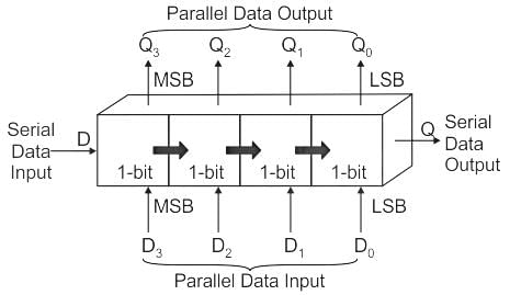
The structure of the SIPO register is:
Basic data movement in a shift register is shown below:
Calculation
Given that the initial content is 0000 and the data is 1101.
After the first clock pulse, the value of the register is 1000.
After the second clock pulse, the value of the register is 0100.
After the third clock pulse, the value of the register is 1010.
After the fourth clock pulse, the value of the register is 1101.
A D flip-flop can be constructed from an ______ flip-flop.- a)S-R
- b)J-K
- c)T
- d)S-K
Correct answer is option 'A'. Can you explain this answer?
A D flip-flop can be constructed from an ______ flip-flop.
a)
S-R
b)
J-K
c)
T
d)
S-K
|
|
Pooja Patel answered |
A D flip-flop can be constructed from an S-R flip-flop by inserting an inverter between S and R and assigning the symbol D to the S input.
What is one disadvantage of an S-R flip-flop ?- a)It has no Enable input
- b)It has a RACE condition
- c)It has no clock input
- d)It has only single output
Correct answer is option 'B'. Can you explain this answer?
What is one disadvantage of an S-R flip-flop ?
a)
It has no Enable input
b)
It has a RACE condition
c)
It has no clock input
d)
It has only single output
|
|
Sharmila Bajaj answered |
Disadvantage of S-R Flip-Flop: Race Condition
The S-R (Set-Reset) flip-flop is a fundamental memory element in digital electronics. However, it comes with a significant disadvantage known as the race condition.
Understanding Race Condition
- Definition: A race condition occurs when the output of a flip-flop depends on the sequence or timing of input signals. In the case of an S-R flip-flop, this can lead to unpredictable behavior.
- Scenario: If both the Set (S) and Reset (R) inputs are activated simultaneously (S=1 and R=1), the flip-flop enters an indeterminate state. This situation can cause the outputs to toggle unpredictably, leading to system instability.
Implications of Race Condition
- Unstable Output: The primary outcome of a race condition is that the output may not settle to a stable state, which can cause errors in digital circuits.
- Design Complexity: To mitigate this issue, designers may need to implement additional circuitry, such as using clocked flip-flops or incorporating external controls, complicating the design process.
Comparison with Other Options
- No Enable Input: While the S-R flip-flop lacks an enable input, this is not inherently problematic for all applications.
- No Clock Input: The absence of a clock input can limit its functionality but is not as critical as the race condition.
- Single Output: Having only a single output is a design choice and does not represent a flaw in functionality.
In conclusion, while S-R flip-flops are useful in many applications, the presence of race conditions significantly undermines their reliability, making it a key disadvantage to consider in digital design.
An 8-bit serial in/serial out shift register is used with a clock frequency of 2 MHz to achieve a time delay (td) of ________- a)16 us
- b)8 us
- c)4 us
- d)2 us
Correct answer is option 'C'. Can you explain this answer?
An 8-bit serial in/serial out shift register is used with a clock frequency of 2 MHz to achieve a time delay (td) of ________
a)
16 us
b)
8 us
c)
4 us
d)
2 us
|
|
Pooja Patel answered |
One clock period is = (1⁄2) micro-s = 0.5 microseconds. In serial transmission, data enters one bit at a time.
So, the total delay = 0.5 x 8 = 4 micro seconds time is required to transmit information of 8 bits.
So, the total delay = 0.5 x 8 = 4 micro seconds time is required to transmit information of 8 bits.
A synchronous counter using two J – K flip flops that goes through the sequence of states: Q1 Q2 = 00 → 10 → 01 → 11 → 00 …. is required. To achieve this, the inputs to the flip flops are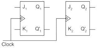
- a)J1 = Q2, K1 = 0; J2 = Q1’, K2 = Q1
- b)J1 = 1, K1 = 1; J2 = Q1, K2 = Q1
- c)J1 = Q2, K1 = Q2’; J2 = 1, K2 = 1
- d)J1 = Q2’, K1 = Q2; J2 = Q1, K2 = Q1’
Correct answer is option 'B'. Can you explain this answer?
A synchronous counter using two J – K flip flops that goes through the sequence of states: Q1 Q2 = 00 → 10 → 01 → 11 → 00 …. is required. To achieve this, the inputs to the flip flops are
a)
J1 = Q2, K1 = 0; J2 = Q1’, K2 = Q1
b)
J1 = 1, K1 = 1; J2 = Q1, K2 = Q1
c)
J1 = Q2, K1 = Q2’; J2 = 1, K2 = 1
d)
J1 = Q2’, K1 = Q2; J2 = Q1, K2 = Q1’
|
|
Pooja Patel answered |
By using excitation table of JK flip flop.
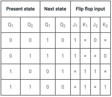
From the above table,
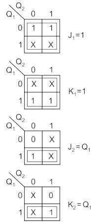
S-R type flip-flop can be converted into D type flip-flop if S is connected to R through ____________- a)OR Gate
- b)AND Gate
- c)Inverter
- d)Full Adder
Correct answer is option 'C'. Can you explain this answer?
S-R type flip-flop can be converted into D type flip-flop if S is connected to R through ____________
a)
OR Gate
b)
AND Gate
c)
Inverter
d)
Full Adder
|
|
Pooja Patel answered |
S-R type flip-flop can be converted into D type flip-flop if S is connected to R through an Inverter gate.
In the latch circuit shown, the NAND gates have non-zero, but unequal propagation delays. The present input conditions is: P = Q = ‘0’. If the input conditions is changed simultaneously to P = Q = ‘1’, the outputs X and Y are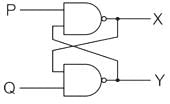
- a)X = ‘1’, Y = ‘1’
- b)either X = ‘1’, Y = ‘0’ or X = ‘0’, Y = ‘1’
- c)either X = ‘1’, Y = ‘1’ or X = ‘0’, Y = ‘0’
- d)X = ‘0’, Y = ‘0’
Correct answer is option 'B'. Can you explain this answer?
In the latch circuit shown, the NAND gates have non-zero, but unequal propagation delays. The present input conditions is: P = Q = ‘0’. If the input conditions is changed simultaneously to P = Q = ‘1’, the outputs X and Y are
a)
X = ‘1’, Y = ‘1’
b)
either X = ‘1’, Y = ‘0’ or X = ‘0’, Y = ‘1’
c)
either X = ‘1’, Y = ‘1’ or X = ‘0’, Y = ‘0’
d)
X = ‘0’, Y = ‘0’
|
|
Pioneer Academy answered |
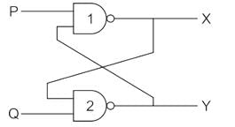
Let as assume tpd 1 < tpd 2
x changes state first then y changes
1st output of X (P = 1, y = 0) ⇒ X1 = 1
Next output of Y (Q = 1, X1 = 1) ⇒ Y1 = 0
2nd output of X (P = 1, y1 = 0) ⇒ 1
Hence output x = 1 y = 0 (if tpd1 < tpd2)
& Output X = 0 Y = 1 (if tpd2 < tpd1)
One of the major drawbacks to the use of asynchronous counters is that ____________- a)Low-frequency applications are limited because of internal propagation delays
- b)High-frequency applications are limited because of internal propagation delays
- c)Asynchronous counters do not have major drawbacks and are suitable for use in high- and low-frequency counting applications
- d)Asynchronous counters do not have propagation delays, which limits their use in high-frequency applications
Correct answer is option 'B'. Can you explain this answer?
One of the major drawbacks to the use of asynchronous counters is that ____________
a)
Low-frequency applications are limited because of internal propagation delays
b)
High-frequency applications are limited because of internal propagation delays
c)
Asynchronous counters do not have major drawbacks and are suitable for use in high- and low-frequency counting applications
d)
Asynchronous counters do not have propagation delays, which limits their use in high-frequency applications
|
|
Naveen Kapoor answered |
Introduction:
Asynchronous counters are a type of digital circuit that can count events or perform other operations based on clock signals. While they offer advantages such as simplicity and low power consumption, they also have some drawbacks that limit their use in certain applications.
Explanation:
The major drawback of using asynchronous counters is that high-frequency applications are limited because of internal propagation delays. Let's understand this in detail:
1. Asynchronous Counters:
- Asynchronous counters, also known as ripple counters, are made up of a series of flip-flops connected in a cascaded manner.
- Each flip-flop in the counter divides the frequency of the clock signal by 2.
- The output of one flip-flop serves as the clock input for the next flip-flop in the sequence, creating a ripple effect.
- As a result, the outputs of the flip-flops change sequentially, resulting in a binary count.
2. Propagation Delay:
- Propagation delay refers to the time it takes for a signal to travel through a digital circuit from input to output.
- In the case of asynchronous counters, the propagation delay is the time it takes for a change in the input signal to propagate through the flip-flops and reach the output.
- This delay is caused by the internal logic gates used in the flip-flops, which introduce a certain amount of delay.
3. High-Frequency Limitation:
- The internal propagation delays in asynchronous counters create a limitation for high-frequency applications.
- As the clock frequency increases, the propagation delay becomes more significant.
- At high frequencies, the output of each flip-flop may not have enough time to settle before the next clock pulse arrives.
- This can result in incorrect counting and unpredictable behavior of the counter.
Conclusion:
In conclusion, the major drawback of using asynchronous counters is the limitation they impose on high-frequency applications due to internal propagation delays. While they are suitable for low-frequency counting applications, their use becomes less reliable and predictable at higher frequencies.
A feature that distinguishes the JK flip flop from the SR flip flop is the- a)Toggle condition
- b)Preset input
- c)Type of clock
- d)Clear input
Correct answer is option 'A'. Can you explain this answer?
A feature that distinguishes the JK flip flop from the SR flip flop is the
a)
Toggle condition
b)
Preset input
c)
Type of clock
d)
Clear input
|
|
Pooja Patel answered |
In J-K flip flop when both inputs are HIGH, the output toggles i.e. it changes from high to low and low to high periodically when both the inputs are 1.
For an SR flip flop, however, when both the inputs are HIGH, we encounter an invalid state, which is not present for a JK flip flop.
This is explained with the help of the following function table:
For an SR flip flop, however, when both the inputs are HIGH, we encounter an invalid state, which is not present for a JK flip flop.
This is explained with the help of the following function table:
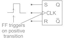

Similarly, for a JK flip flop, the block diagram along with the function table is as shown:
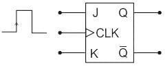
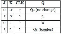
Features that distinguish:
a) When both S and R inputs are 1, output goes to a metastable state but when both the inputs of J and K are 1 output is in toggle state with respect to the previous state.
b) JK flip flop is often termed as Universal flip flop because all other flips like D, T, and SR can be derived from that while this is not the case with respect to SR flip flops.
c) SR flip flops when used as latch can be helpful in the bounce elimination of the switches which is one of its major advantages while this is not the case with JK flip flops.
For SR flip-flop with NOR gates, the undefined state is- a)S = 0, R = 0
- b)S = 0, R = 1
- c)S = 1, R = 1
- d)S = 1, R = 0
Correct answer is option 'C'. Can you explain this answer?
For SR flip-flop with NOR gates, the undefined state is
a)
S = 0, R = 0
b)
S = 0, R = 1
c)
S = 1, R = 1
d)
S = 1, R = 0
|
|
Pooja Patel answered |
An un-clocked R-S flip flop using NOR gates is as shown:

The truth table for the circuit is shown:

In which of the following condition the SR flip flop are unstable?- a)S = 0, R = 1
- b)S = 1, R = 0
- c)S = 0, R = 0
- d)S = 1, R = 1
Correct answer is option 'D'. Can you explain this answer?
In which of the following condition the SR flip flop are unstable?
a)
S = 0, R = 1
b)
S = 1, R = 0
c)
S = 0, R = 0
d)
S = 1, R = 1
|
|
Upasana Joshi answered |
SR Flip Flop Stability
The SR flip flop is a basic type of flip flop that consists of two inputs, S (Set) and R (Reset), and two outputs, Q (Output) and Q' (Inverted Output). It is used to store one bit of information and can be triggered by a clock signal.
Stability of SR Flip Flop
The stability of an SR flip flop refers to its ability to maintain a stable output state when the inputs are changed. In other words, a stable flip flop should not change its output state when the inputs are changed.
Explanation of Options
a) S = 0, R = 1:
In this case, the Set input S is 0 and the Reset input R is 1. When the Set input is 0 and the Reset input is 1, the flip flop enters an unstable state. This is because both inputs are active, which violates the normal operation of the flip flop. The output state becomes unpredictable, and it may toggle between different states or remain in an undefined state.
b) S = 1, R = 0:
In this case, the Set input S is 1 and the Reset input R is 0. When the Set input is 1 and the Reset input is 0, the flip flop enters an unstable state. This is again because both inputs are active, violating the normal operation of the flip flop. The output state becomes unpredictable and may toggle between different states or remain in an undefined state.
c) S = 0, R = 0:
In this case, both the Set input S and the Reset input R are 0. When both inputs are 0, the flip flop remains in its current state. The output state does not change, and the flip flop remains stable.
d) S = 1, R = 1:
In this case, both the Set input S and the Reset input R are 1. When both inputs are 1, the flip flop enters an unstable state. This is because both inputs are active, violating the normal operation of the flip flop. The output state becomes unpredictable and may toggle between different states or remain in an undefined state.
Conclusion
The SR flip flop is unstable when both the Set and Reset inputs are 1 (Option D). In this case, the flip flop enters an unpredictable state, and the output may toggle or remain undefined. Therefore, the correct answer is option D.
Which of the following is correct for a gated D flip-flop?- a)The output toggles if one of the inputs is held HIGH
- b)Only one of the inputs can be HIGH at a time
- c)The output complement follows the input when enabled
- d)Q output follows the input D when the enable is HIGH
Correct answer is option 'D'. Can you explain this answer?
Which of the following is correct for a gated D flip-flop?
a)
The output toggles if one of the inputs is held HIGH
b)
Only one of the inputs can be HIGH at a time
c)
The output complement follows the input when enabled
d)
Q output follows the input D when the enable is HIGH
|
|
Pooja Patel answered |
If clock is high then the D flip-flop operate and we know that input is equals to output in case of D flip-flop. It stores the value on the data line.
The functional difference between SR flip-flop and JK flip-flop is that- a)JK flip-flop is faster than SR flip-flop
- b)JK flip-flop has a feedback path
- c)JK flip-flop accepts both inputs 1
- d)None of the above
Correct answer is option 'C'. Can you explain this answer?
The functional difference between SR flip-flop and JK flip-flop is that
a)
JK flip-flop is faster than SR flip-flop
b)
JK flip-flop has a feedback path
c)
JK flip-flop accepts both inputs 1
d)
None of the above
|
|
Pooja Patel answered |
In J-K flip flop when both inputs are HIGH, the output toggles i.e. it changes from high to low and low to high periodically when both the inputs are 1.
For an SR flip flop, however, when both the inputs are HIGH, we encounter an invalid state, which is not present for a JK flip flop.
This is explained with the help of the following function table:
For an SR flip flop, however, when both the inputs are HIGH, we encounter an invalid state, which is not present for a JK flip flop.
This is explained with the help of the following function table:


Similarly, for a JK flip flop, the block diagram along with the function table is as shown:


Input clock of RS flip-flop is given to ____________- a)Input
- b)Pulser
- c)Output
- d)Master slave flip-flop
Correct answer is option 'B'. Can you explain this answer?
Input clock of RS flip-flop is given to ____________
a)
Input
b)
Pulser
c)
Output
d)
Master slave flip-flop
|
|
Pooja Patel answered |
Pulser behaves like an arithmetic operator, to perform the operation or determination of corresponding states.
Chapter doubts & questions for Sequential Circuits - Digital Electronics 2025 is part of Electrical Engineering (EE) exam preparation. The chapters have been prepared according to the Electrical Engineering (EE) exam syllabus. The Chapter doubts & questions, notes, tests & MCQs are made for Electrical Engineering (EE) 2025 Exam. Find important definitions, questions, notes, meanings, examples, exercises, MCQs and online tests here.
Chapter doubts & questions of Sequential Circuits - Digital Electronics in English & Hindi are available as part of Electrical Engineering (EE) exam.
Download more important topics, notes, lectures and mock test series for Electrical Engineering (EE) Exam by signing up for free.
Digital Electronics
115 videos|71 docs|58 tests
|

Signup to see your scores go up within 7 days!
Study with 1000+ FREE Docs, Videos & Tests
10M+ students study on EduRev
|
© EduRev
|
Education Revolution
|


|


Signup to see your scores
go up
within 7 days!
within 7 days!
Takes less than 10 seconds to signup