Electronics and Communication Engineering (ECE) Exam > Electronics and Communication Engineering (ECE) Questions > In the circuit shown, the threshold voltages ...
Start Learning for Free
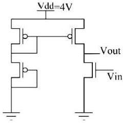
In the circuit shown, the threshold voltages of the pMOS (|Vtp|) and nMOS (Vtn) transistors are both equal to 1 V. All the transistors have the same output resistance rds of 6 MΩ. The other parameters are listed below.

Μn and μp are the carrier mobilites, and Cox is the oxide capacitance per unit area. Ignoring the effect of channel length modulation and body bias, the gain of the circuit is ____________(rounded off to 1 decimal place).

Correct answer is '-900'. Can you explain this answer?
| FREE This question is part of | Download PDF Attempt this Test |
Verified Answer
In the circuit shown, the threshold voltages of the pMOS (|Vtp|) and n...


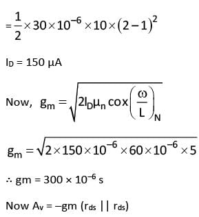
= –300 × 10–6 × 3 × 106
∴ AV = –900
∴ AV = –900

|
Explore Courses for Electronics and Communication Engineering (ECE) exam
|

|
Similar Electronics and Communication Engineering (ECE) Doubts
In the circuit shown, the threshold voltages of the pMOS (|Vtp|) and nMOS (Vtn) transistors are both equal to 1 V. All the transistors have the same output resistance rds of 6 MΩ. The other parameters are listed below.Μn and μp are the carrier mobilites, and Cox is the oxide capacitance per unit area. Ignoring the effect of channel length modulation and body bias, the gain of the circuit is ____________(rounded off to 1 decimal place).Correct answer is '-900'. Can you explain this answer?
Question Description
In the circuit shown, the threshold voltages of the pMOS (|Vtp|) and nMOS (Vtn) transistors are both equal to 1 V. All the transistors have the same output resistance rds of 6 MΩ. The other parameters are listed below.Μn and μp are the carrier mobilites, and Cox is the oxide capacitance per unit area. Ignoring the effect of channel length modulation and body bias, the gain of the circuit is ____________(rounded off to 1 decimal place).Correct answer is '-900'. Can you explain this answer? for Electronics and Communication Engineering (ECE) 2024 is part of Electronics and Communication Engineering (ECE) preparation. The Question and answers have been prepared according to the Electronics and Communication Engineering (ECE) exam syllabus. Information about In the circuit shown, the threshold voltages of the pMOS (|Vtp|) and nMOS (Vtn) transistors are both equal to 1 V. All the transistors have the same output resistance rds of 6 MΩ. The other parameters are listed below.Μn and μp are the carrier mobilites, and Cox is the oxide capacitance per unit area. Ignoring the effect of channel length modulation and body bias, the gain of the circuit is ____________(rounded off to 1 decimal place).Correct answer is '-900'. Can you explain this answer? covers all topics & solutions for Electronics and Communication Engineering (ECE) 2024 Exam. Find important definitions, questions, meanings, examples, exercises and tests below for In the circuit shown, the threshold voltages of the pMOS (|Vtp|) and nMOS (Vtn) transistors are both equal to 1 V. All the transistors have the same output resistance rds of 6 MΩ. The other parameters are listed below.Μn and μp are the carrier mobilites, and Cox is the oxide capacitance per unit area. Ignoring the effect of channel length modulation and body bias, the gain of the circuit is ____________(rounded off to 1 decimal place).Correct answer is '-900'. Can you explain this answer?.
In the circuit shown, the threshold voltages of the pMOS (|Vtp|) and nMOS (Vtn) transistors are both equal to 1 V. All the transistors have the same output resistance rds of 6 MΩ. The other parameters are listed below.Μn and μp are the carrier mobilites, and Cox is the oxide capacitance per unit area. Ignoring the effect of channel length modulation and body bias, the gain of the circuit is ____________(rounded off to 1 decimal place).Correct answer is '-900'. Can you explain this answer? for Electronics and Communication Engineering (ECE) 2024 is part of Electronics and Communication Engineering (ECE) preparation. The Question and answers have been prepared according to the Electronics and Communication Engineering (ECE) exam syllabus. Information about In the circuit shown, the threshold voltages of the pMOS (|Vtp|) and nMOS (Vtn) transistors are both equal to 1 V. All the transistors have the same output resistance rds of 6 MΩ. The other parameters are listed below.Μn and μp are the carrier mobilites, and Cox is the oxide capacitance per unit area. Ignoring the effect of channel length modulation and body bias, the gain of the circuit is ____________(rounded off to 1 decimal place).Correct answer is '-900'. Can you explain this answer? covers all topics & solutions for Electronics and Communication Engineering (ECE) 2024 Exam. Find important definitions, questions, meanings, examples, exercises and tests below for In the circuit shown, the threshold voltages of the pMOS (|Vtp|) and nMOS (Vtn) transistors are both equal to 1 V. All the transistors have the same output resistance rds of 6 MΩ. The other parameters are listed below.Μn and μp are the carrier mobilites, and Cox is the oxide capacitance per unit area. Ignoring the effect of channel length modulation and body bias, the gain of the circuit is ____________(rounded off to 1 decimal place).Correct answer is '-900'. Can you explain this answer?.
Solutions for In the circuit shown, the threshold voltages of the pMOS (|Vtp|) and nMOS (Vtn) transistors are both equal to 1 V. All the transistors have the same output resistance rds of 6 MΩ. The other parameters are listed below.Μn and μp are the carrier mobilites, and Cox is the oxide capacitance per unit area. Ignoring the effect of channel length modulation and body bias, the gain of the circuit is ____________(rounded off to 1 decimal place).Correct answer is '-900'. Can you explain this answer? in English & in Hindi are available as part of our courses for Electronics and Communication Engineering (ECE).
Download more important topics, notes, lectures and mock test series for Electronics and Communication Engineering (ECE) Exam by signing up for free.
Here you can find the meaning of In the circuit shown, the threshold voltages of the pMOS (|Vtp|) and nMOS (Vtn) transistors are both equal to 1 V. All the transistors have the same output resistance rds of 6 MΩ. The other parameters are listed below.Μn and μp are the carrier mobilites, and Cox is the oxide capacitance per unit area. Ignoring the effect of channel length modulation and body bias, the gain of the circuit is ____________(rounded off to 1 decimal place).Correct answer is '-900'. Can you explain this answer? defined & explained in the simplest way possible. Besides giving the explanation of
In the circuit shown, the threshold voltages of the pMOS (|Vtp|) and nMOS (Vtn) transistors are both equal to 1 V. All the transistors have the same output resistance rds of 6 MΩ. The other parameters are listed below.Μn and μp are the carrier mobilites, and Cox is the oxide capacitance per unit area. Ignoring the effect of channel length modulation and body bias, the gain of the circuit is ____________(rounded off to 1 decimal place).Correct answer is '-900'. Can you explain this answer?, a detailed solution for In the circuit shown, the threshold voltages of the pMOS (|Vtp|) and nMOS (Vtn) transistors are both equal to 1 V. All the transistors have the same output resistance rds of 6 MΩ. The other parameters are listed below.Μn and μp are the carrier mobilites, and Cox is the oxide capacitance per unit area. Ignoring the effect of channel length modulation and body bias, the gain of the circuit is ____________(rounded off to 1 decimal place).Correct answer is '-900'. Can you explain this answer? has been provided alongside types of In the circuit shown, the threshold voltages of the pMOS (|Vtp|) and nMOS (Vtn) transistors are both equal to 1 V. All the transistors have the same output resistance rds of 6 MΩ. The other parameters are listed below.Μn and μp are the carrier mobilites, and Cox is the oxide capacitance per unit area. Ignoring the effect of channel length modulation and body bias, the gain of the circuit is ____________(rounded off to 1 decimal place).Correct answer is '-900'. Can you explain this answer? theory, EduRev gives you an
ample number of questions to practice In the circuit shown, the threshold voltages of the pMOS (|Vtp|) and nMOS (Vtn) transistors are both equal to 1 V. All the transistors have the same output resistance rds of 6 MΩ. The other parameters are listed below.Μn and μp are the carrier mobilites, and Cox is the oxide capacitance per unit area. Ignoring the effect of channel length modulation and body bias, the gain of the circuit is ____________(rounded off to 1 decimal place).Correct answer is '-900'. Can you explain this answer? tests, examples and also practice Electronics and Communication Engineering (ECE) tests.

|
Explore Courses for Electronics and Communication Engineering (ECE) exam
|

|
Suggested Free Tests
Signup for Free!
Signup to see your scores go up within 7 days! Learn & Practice with 1000+ FREE Notes, Videos & Tests.


