Electronics and Communication Engineering (ECE) Exam > Electronics and Communication Engineering (ECE) Questions > Consider the circuit shown with an ideal lon...
Start Learning for Free
Consider the circuit shown with an ideal long channel nMOSFET (enhancement-mode, substrate is connected to the source). The transistor is appropriately biased in the saturation region with VGG and VDD such that it acts as a linear amplifier. vi is the small-signal ac input voltage. vA and vB represent the small-signal voltages at the nodes A and B, respectively. The value of vA/vB is _______. (round off to one decimal place)
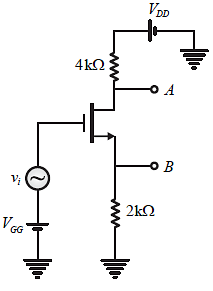
- a)-1.9
- b)-2.1
Correct answer is between '-1.9,-2.1'. Can you explain this answer?
| FREE This question is part of | Download PDF Attempt this Test |
Most Upvoted Answer
Consider the circuit shown with an ideal long channel nMOSFET (enhanc...
Method 1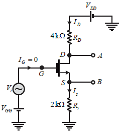





Given circuit is shown below,

From above figure,
IG = 0
So, ID = IS
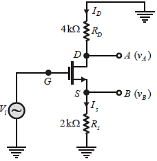
AC equivalent circuit :
(i) All capacitors are short circuited.
(ii) All DC voltage sources are replaced by short circuit.
(iii)All DC current sources are replaced by open circuit.

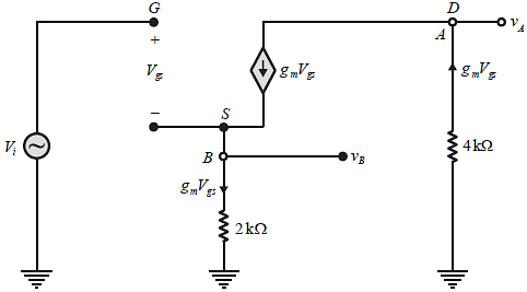
Small signal equivalent circuit is shown below,

Voltage at A, vA = -RDgmVgs ………..(i)
Voltage at B, vB = RsgmVgs ……..(ii)

Hence, the correct answer is – 2.
Method 2
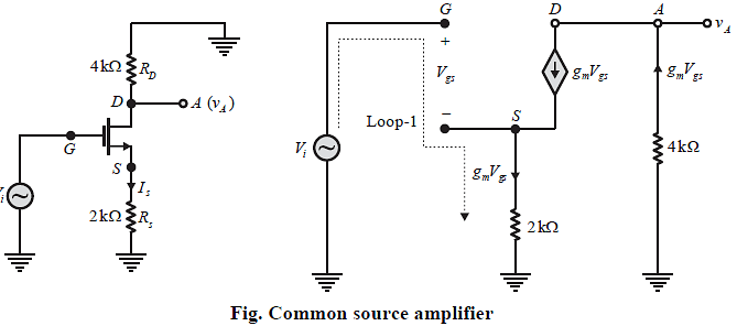
Case 1 : Consider output at point-A only i.e. vA , so given circuit behave as common source amplifier ,whose small signal equivalent circuit is shown below,

Apply KVL in loop-1,

Voltage at point-A is,

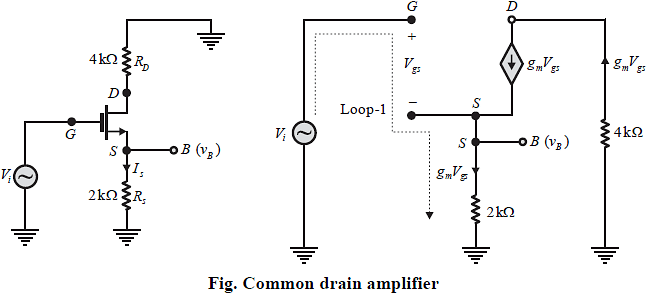
Case 2 : Consider output at point-B only i.e. vB so given circuit behave as common drain amplifier, whose
small signal equivalent circuit is shown below,

Apply KVL is loop-1,

Voltage at point-B,

From equation (iii) and (vi),

Hence, the correct answer is – 2.
Free Test
FREE
| Start Free Test |
Community Answer
Consider the circuit shown with an ideal long channel nMOSFET (enhanc...
Method 1


Given circuit is shown below,

From above figure,
IG = 0
So, ID = IS
AC equivalent circuit :
(i) All capacitors are short circuited.
(ii) All DC voltage sources are replaced by short circuit.
(iii)All DC current sources are replaced by open circuit.

Small signal equivalent circuit is shown below,

Voltage at A, vA = -RDgmVgs ………..(i)
Voltage at B, vB = RsgmVgs ……..(ii)

Hence, the correct answer is – 2.
Method 2
Case 1 : Consider output at point-A only i.e. vA , so given circuit behave as common source amplifier ,whose small signal equivalent circuit is shown below,

Apply KVL in loop-1,

Voltage at point-A is,

Case 2 : Consider output at point-B only i.e. vB so given circuit behave as common drain amplifier, whose
small signal equivalent circuit is shown below,

Apply KVL is loop-1,

Voltage at point-B,

From equation (iii) and (vi),

Hence, the correct answer is – 2.
Attention Electronics and Communication Engineering (ECE) Students!
To make sure you are not studying endlessly, EduRev has designed Electronics and Communication Engineering (ECE) study material, with Structured Courses, Videos, & Test Series. Plus get personalized analysis, doubt solving and improvement plans to achieve a great score in Electronics and Communication Engineering (ECE).

|
Explore Courses for Electronics and Communication Engineering (ECE) exam
|

|
Similar Electronics and Communication Engineering (ECE) Doubts
Consider the circuit shown with an ideal long channel nMOSFET (enhancement-mode, substrate is connected to the source). The transistor is appropriately biased in the saturation region with VGG and VDD such that it acts as a linear amplifier. vi is the small-signal ac input voltage. vA and vB represent the small-signal voltages at the nodes A and B, respectively. The value of vA/vB is _______. (round off to one decimal place)a)-1.9b)-2.1Correct answer is between '-1.9,-2.1'. Can you explain this answer?
Question Description
Consider the circuit shown with an ideal long channel nMOSFET (enhancement-mode, substrate is connected to the source). The transistor is appropriately biased in the saturation region with VGG and VDD such that it acts as a linear amplifier. vi is the small-signal ac input voltage. vA and vB represent the small-signal voltages at the nodes A and B, respectively. The value of vA/vB is _______. (round off to one decimal place)a)-1.9b)-2.1Correct answer is between '-1.9,-2.1'. Can you explain this answer? for Electronics and Communication Engineering (ECE) 2024 is part of Electronics and Communication Engineering (ECE) preparation. The Question and answers have been prepared according to the Electronics and Communication Engineering (ECE) exam syllabus. Information about Consider the circuit shown with an ideal long channel nMOSFET (enhancement-mode, substrate is connected to the source). The transistor is appropriately biased in the saturation region with VGG and VDD such that it acts as a linear amplifier. vi is the small-signal ac input voltage. vA and vB represent the small-signal voltages at the nodes A and B, respectively. The value of vA/vB is _______. (round off to one decimal place)a)-1.9b)-2.1Correct answer is between '-1.9,-2.1'. Can you explain this answer? covers all topics & solutions for Electronics and Communication Engineering (ECE) 2024 Exam. Find important definitions, questions, meanings, examples, exercises and tests below for Consider the circuit shown with an ideal long channel nMOSFET (enhancement-mode, substrate is connected to the source). The transistor is appropriately biased in the saturation region with VGG and VDD such that it acts as a linear amplifier. vi is the small-signal ac input voltage. vA and vB represent the small-signal voltages at the nodes A and B, respectively. The value of vA/vB is _______. (round off to one decimal place)a)-1.9b)-2.1Correct answer is between '-1.9,-2.1'. Can you explain this answer?.
Consider the circuit shown with an ideal long channel nMOSFET (enhancement-mode, substrate is connected to the source). The transistor is appropriately biased in the saturation region with VGG and VDD such that it acts as a linear amplifier. vi is the small-signal ac input voltage. vA and vB represent the small-signal voltages at the nodes A and B, respectively. The value of vA/vB is _______. (round off to one decimal place)a)-1.9b)-2.1Correct answer is between '-1.9,-2.1'. Can you explain this answer? for Electronics and Communication Engineering (ECE) 2024 is part of Electronics and Communication Engineering (ECE) preparation. The Question and answers have been prepared according to the Electronics and Communication Engineering (ECE) exam syllabus. Information about Consider the circuit shown with an ideal long channel nMOSFET (enhancement-mode, substrate is connected to the source). The transistor is appropriately biased in the saturation region with VGG and VDD such that it acts as a linear amplifier. vi is the small-signal ac input voltage. vA and vB represent the small-signal voltages at the nodes A and B, respectively. The value of vA/vB is _______. (round off to one decimal place)a)-1.9b)-2.1Correct answer is between '-1.9,-2.1'. Can you explain this answer? covers all topics & solutions for Electronics and Communication Engineering (ECE) 2024 Exam. Find important definitions, questions, meanings, examples, exercises and tests below for Consider the circuit shown with an ideal long channel nMOSFET (enhancement-mode, substrate is connected to the source). The transistor is appropriately biased in the saturation region with VGG and VDD such that it acts as a linear amplifier. vi is the small-signal ac input voltage. vA and vB represent the small-signal voltages at the nodes A and B, respectively. The value of vA/vB is _______. (round off to one decimal place)a)-1.9b)-2.1Correct answer is between '-1.9,-2.1'. Can you explain this answer?.
Solutions for Consider the circuit shown with an ideal long channel nMOSFET (enhancement-mode, substrate is connected to the source). The transistor is appropriately biased in the saturation region with VGG and VDD such that it acts as a linear amplifier. vi is the small-signal ac input voltage. vA and vB represent the small-signal voltages at the nodes A and B, respectively. The value of vA/vB is _______. (round off to one decimal place)a)-1.9b)-2.1Correct answer is between '-1.9,-2.1'. Can you explain this answer? in English & in Hindi are available as part of our courses for Electronics and Communication Engineering (ECE).
Download more important topics, notes, lectures and mock test series for Electronics and Communication Engineering (ECE) Exam by signing up for free.
Here you can find the meaning of Consider the circuit shown with an ideal long channel nMOSFET (enhancement-mode, substrate is connected to the source). The transistor is appropriately biased in the saturation region with VGG and VDD such that it acts as a linear amplifier. vi is the small-signal ac input voltage. vA and vB represent the small-signal voltages at the nodes A and B, respectively. The value of vA/vB is _______. (round off to one decimal place)a)-1.9b)-2.1Correct answer is between '-1.9,-2.1'. Can you explain this answer? defined & explained in the simplest way possible. Besides giving the explanation of
Consider the circuit shown with an ideal long channel nMOSFET (enhancement-mode, substrate is connected to the source). The transistor is appropriately biased in the saturation region with VGG and VDD such that it acts as a linear amplifier. vi is the small-signal ac input voltage. vA and vB represent the small-signal voltages at the nodes A and B, respectively. The value of vA/vB is _______. (round off to one decimal place)a)-1.9b)-2.1Correct answer is between '-1.9,-2.1'. Can you explain this answer?, a detailed solution for Consider the circuit shown with an ideal long channel nMOSFET (enhancement-mode, substrate is connected to the source). The transistor is appropriately biased in the saturation region with VGG and VDD such that it acts as a linear amplifier. vi is the small-signal ac input voltage. vA and vB represent the small-signal voltages at the nodes A and B, respectively. The value of vA/vB is _______. (round off to one decimal place)a)-1.9b)-2.1Correct answer is between '-1.9,-2.1'. Can you explain this answer? has been provided alongside types of Consider the circuit shown with an ideal long channel nMOSFET (enhancement-mode, substrate is connected to the source). The transistor is appropriately biased in the saturation region with VGG and VDD such that it acts as a linear amplifier. vi is the small-signal ac input voltage. vA and vB represent the small-signal voltages at the nodes A and B, respectively. The value of vA/vB is _______. (round off to one decimal place)a)-1.9b)-2.1Correct answer is between '-1.9,-2.1'. Can you explain this answer? theory, EduRev gives you an
ample number of questions to practice Consider the circuit shown with an ideal long channel nMOSFET (enhancement-mode, substrate is connected to the source). The transistor is appropriately biased in the saturation region with VGG and VDD such that it acts as a linear amplifier. vi is the small-signal ac input voltage. vA and vB represent the small-signal voltages at the nodes A and B, respectively. The value of vA/vB is _______. (round off to one decimal place)a)-1.9b)-2.1Correct answer is between '-1.9,-2.1'. Can you explain this answer? tests, examples and also practice Electronics and Communication Engineering (ECE) tests.

|
Explore Courses for Electronics and Communication Engineering (ECE) exam
|

|
Suggested Free Tests
Signup for Free!
Signup to see your scores go up within 7 days! Learn & Practice with 1000+ FREE Notes, Videos & Tests.


