


All Exams >
UPSC >
Electrical Engineering Optional Notes for UPSC >
All Questions
All questions of Principles of Thyristor Choppers and Inverters for UPSC CSE Exam
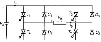
In current source inverters load voltage waveform V0 and load current waveform i0 respectively- a)depends on load impedance Z, does not depends on Z.
- b)depends on Z, depends on Z.
- c)does not depend on Z, does not depend on Z.
- d)does not depend on Z, depends on Z.
Correct answer is option 'A'. Can you explain this answer?
In current source inverters load voltage waveform V0 and load current waveform i0 respectively
a)
depends on load impedance Z, does not depends on Z.
b)
depends on Z, depends on Z.
c)
does not depend on Z, does not depend on Z.
d)
does not depend on Z, depends on Z.
|
|
Pankaj Mehta answered |
In a CSI, load current rather than load voltage is controlled, and the inverter output voltage is dependent upon the load impedance and the output voltage waveform. The load current and hence its waveform is independent of load impedance due to which a CSI has inherent protection against short-circuit across its terminals.

If T is the chopping period, Ton the on-time period of chopper and Toff the off-time period of the chopper, then consider the following statements associated with the methods of controlling the output voltage of a chopper:
1. In pulse-width modulation (PWM) scheme, T is kept constant while Ton is varied.
2. In variable-frequency modulation (VFM) scheme, T is varied while either of Ton or Toff is kept constant.
3. In PWM scheme, the output voltage can be varied between zero to source voltage.
4. The large Toff in VFM scheme may make the load current discontinuous
5. PWM scheme is better than VFM scheme.Which of the statements given above are correct?- a)1,2,3, 4, and 5
- b)2, 3 and 5
- c)1,3 and 4
- d)2, 3, 4 and 5
Correct answer is option 'A'. Can you explain this answer?
If T is the chopping period, Ton the on-time period of chopper and Toff the off-time period of the chopper, then consider the following statements associated with the methods of controlling the output voltage of a chopper:
1. In pulse-width modulation (PWM) scheme, T is kept constant while Ton is varied.
2. In variable-frequency modulation (VFM) scheme, T is varied while either of Ton or Toff is kept constant.
3. In PWM scheme, the output voltage can be varied between zero to source voltage.
4. The large Toff in VFM scheme may make the load current discontinuous
5. PWM scheme is better than VFM scheme.
Which of the statements given above are correct?
a)
1,2,3, 4, and 5
b)
2, 3 and 5
c)
1,3 and 4
d)
2, 3, 4 and 5
|
|
Luminary Institute answered |
For dc – dc converter the critical inductance value.
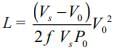
V0 = a Vs = 0.8 × 100 = 80 V
I0 = 2A Power P0 = V0 I0 = 160 Watt
f = 500
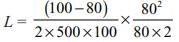
= 8 × 10⁻³ H = 8 mH.
V0 = a Vs = 0.8 × 100 = 80 V
I0 = 2A Power P0 = V0 I0 = 160 Watt
f = 500
= 8 × 10⁻³ H = 8 mH.
Inverters designed from BJT are preferably used in saturation region than in active region because of- a)high efficiency
- b)high power factor
- c)both (a) and (b)
- d)none of these
Correct answer is option 'C'. Can you explain this answer?
Inverters designed from BJT are preferably used in saturation region than in active region because of
a)
high efficiency
b)
high power factor
c)
both (a) and (b)
d)
none of these
|
|
Rajesh Saha answered |
Introduction:
Inverters are electronic devices that convert DC (Direct Current) power into AC (Alternating Current) power. They are widely used in various applications like power supplies, motor drives, renewable energy systems, etc. Inverters can be designed using different types of electronic components, including BJT (Bipolar Junction Transistor).
Active Region vs Saturation Region:
BJTs operate in two main regions - active region and saturation region. In the active region, the BJT acts as an amplifier, and the output voltage is linearly related to the input voltage. In the saturation region, the BJT acts as a switch, and the output voltage is either fully ON (saturated) or fully OFF (cutoff).
Reasons to Prefer Saturation Region:
In the context of inverters designed from BJTs, the saturation region is preferred over the active region due to the following reasons:
1. High Efficiency: In the saturation region, the BJT operates in a fully ON state, which means it has a low resistance. This leads to lower power dissipation and higher efficiency of the inverter. In contrast, in the active region, the BJT operates as an amplifier, which introduces losses and reduces overall efficiency.
2. High Power Factor: Power factor is an important parameter in AC power systems, and it measures the phase relationship between the voltage and current waveforms. In the saturation region, the BJT acts as a switch, and the output waveform closely follows the input waveform, resulting in a power factor close to unity (1). A high power factor is desirable as it reduces reactive power losses and improves the overall system efficiency. On the other hand, in the active region, the BJT operates as an amplifier, which can introduce phase shifts and distortion in the output waveform, leading to a lower power factor.
Conclusion:
Inverters designed from BJTs are preferably used in the saturation region rather than the active region due to their high efficiency and high power factor. The saturation region allows the BJT to operate as a switch, resulting in lower power dissipation, improved efficiency, and a power factor close to unity.
Assertion (A): The lower order harmonics are reduced by using some technique while the higher order harmonics are reduced by using filter.
Reason (R): The cost of the filter is reduced and at the same time transient response is also improved to a great extent.- a)Both A and R are true and R is the correct explanation of A.
- b)Both A and R are true but R is not the correct explanation of A.
- c)A is true but R is false,
- d)A is false but R is true.
Correct answer is option 'A'. Can you explain this answer?
Assertion (A): The lower order harmonics are reduced by using some technique while the higher order harmonics are reduced by using filter.
Reason (R): The cost of the filter is reduced and at the same time transient response is also improved to a great extent.
Reason (R): The cost of the filter is reduced and at the same time transient response is also improved to a great extent.
a)
Both A and R are true and R is the correct explanation of A.
b)
Both A and R are true but R is not the correct explanation of A.
c)
A is true but R is false,
d)
A is false but R is true.
|
|
Luminary Institute answered |
The machine operated at 50 Hz.
Synchronous speed Ns
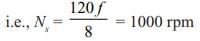
A slip of S = 0.02
Nr = (1 - S) Ns = 980 rpm.
Synchronous speed Ns
A slip of S = 0.02
Nr = (1 - S) Ns = 980 rpm.
In dc choppers, the waveforms for input and output voltages are respectively- a)continuous, discontinuous
- b)both discontinuous
- c)discontinuous, continuous
- d)both continuous
Correct answer is option 'A'. Can you explain this answer?
In dc choppers, the waveforms for input and output voltages are respectively
a)
continuous, discontinuous
b)
both discontinuous
c)
discontinuous, continuous
d)
both continuous
|
|
Prisha Sengupta answered |
Explanation:
DC choppers are electronic devices that are used to convert a fixed DC voltage into a variable DC voltage. The waveform for input and output voltages in DC choppers is as follows:
Input Voltage Waveform:
The input voltage waveform is continuous in DC choppers. It means that the voltage is present at the input of the chopper throughout the operation.
Output Voltage Waveform:
The output voltage waveform is discontinuous in DC choppers. It means that the output voltage is present only for a certain period of time during the operation.
Reason:
The reason for the continuous input voltage waveform is that the input voltage is connected to a DC source that provides a constant voltage. On the other hand, the output voltage waveform is discontinuous because the chopper switches ON and OFF at a certain frequency. During the ON state, the output voltage is present, and during the OFF state, the output voltage is not present.
Conclusion:
Hence, we can conclude that the waveforms for input and output voltages in DC choppers are respectively continuous and discontinuous.
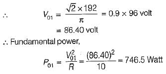
The single-phase half-bridge inverter has a resistive load of 10Ω and the centre-tap dc input voltage is 96 V. The fundamental power consumed by the load is- a)628.6 Watt
- b)525.0Watt'
- c)746.5 Watt
- d)824.4 Watt
Correct answer is option 'C'. Can you explain this answer?
The single-phase half-bridge inverter has a resistive load of 10Ω and the centre-tap dc input voltage is 96 V. The fundamental power consumed by the load is
a)
628.6 Watt
b)
525.0Watt'
c)
746.5 Watt
d)
824.4 Watt
|
|
Niharika Basu answered |
The nth harmonic-component of output voltage is
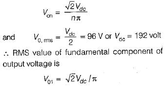
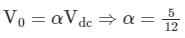
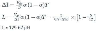
In the circuit shown below, if load R = 500 Ω, switching frequency is 25 kHz and peak to peak ripple current of inductor is limited to 0.9 A then the filter inductance L is

- a)111.62 μH
- b)115.83 μH
- c)136.24 μH
- d)129.62 μH
Correct answer is option 'D'. Can you explain this answer?
In the circuit shown below, if load R = 500 Ω, switching frequency is 25 kHz and peak to peak ripple current of inductor is limited to 0.9 A then the filter inductance L is
a)
111.62 μH
b)
115.83 μH
c)
136.24 μH
d)
129.62 μH
|
|
Luminary Institute answered |
For Buck Converter
The peak to peak ripple current is
The peak to peak ripple current is
A 220 V dc shunt motor runs at 1500 rpm at no-load. The motor is fed through a type-A chopper. If the armature resistance is 1 Ω and duty cycle of chopper is 60%, the speed of the motor when it draw a current of 20 A would be approximately equal to- a)636 rpm
- b)842 rpm
- c)764 rpm
- d)535 rpm
Correct answer is option 'C'. Can you explain this answer?
A 220 V dc shunt motor runs at 1500 rpm at no-load. The motor is fed through a type-A chopper. If the armature resistance is 1 Ω and duty cycle of chopper is 60%, the speed of the motor when it draw a current of 20 A would be approximately equal to
a)
636 rpm
b)
842 rpm
c)
764 rpm
d)
535 rpm
|
|
Aashna Dey answered |
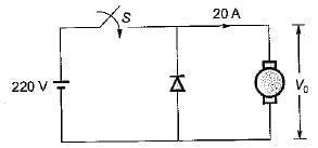
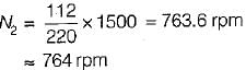
The output voltage,
V0 = αVs = 0.6 x 220 - 132 V
∴ Back emf
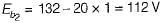
At no- load, N1, = 1500 rpm and Eb1 = 220 V Now, Eb α N
∴

or,
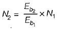
or,
A d.c. chopper circuit connected to a 100 V d.c. source supplies an inductive load having 40 mH in series with a resistance of 5 Ω A freewheeling diode is placed across the load. The load current varies between the limits of 10 A and 12 A. The time ratio (Ton/Toff) of the chopper is- a)1.65
- b)0.98
- c)1.22
- d)0.75
Correct answer is option 'C'. Can you explain this answer?
A d.c. chopper circuit connected to a 100 V d.c. source supplies an inductive load having 40 mH in series with a resistance of 5 Ω A freewheeling diode is placed across the load. The load current varies between the limits of 10 A and 12 A. The time ratio (Ton/Toff) of the chopper is
a)
1.65
b)
0.98
c)
1.22
d)
0.75
|
|
Kiran Iyer answered |
The average value of load current
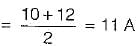
The maximum value of load current
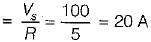
Now, the average value of the voltage is
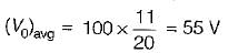
Also,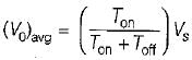
or,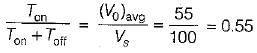
or,
or,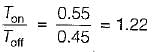
The maximum value of load current
Now, the average value of the voltage is
Also,
or,
or,
or,
A single-phase half bridge inverter has supply voltage of 200 V. For a load resistance of 10 Ω, the output power is equal to- a)2000 W
- b)500 W
- c)225 W
- d)1000W
Correct answer is option 'D'. Can you explain this answer?
A single-phase half bridge inverter has supply voltage of 200 V. For a load resistance of 10 Ω, the output power is equal to
a)
2000 W
b)
500 W
c)
225 W
d)
1000W
|
|
Prisha Sen answered |
Output is a square wave with an amplitude of 100V.
RMS value of a square wave is equal to its peak value.
So, rms value of output voltage is
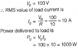
RMS value of a square wave is equal to its peak value.
So, rms value of output voltage is
In chopper circuit the average value of output voltage is controlled by time ratio control (TRC) method. The chopper is operated at a frequency of 5kHz on a 230 V d.c. supply. If the load voltage is 180 V, then the blocking period of thyristor in each cycle is___(in μsec)
Correct answer is between '43,44'. Can you explain this answer?
In chopper circuit the average value of output voltage is controlled by time ratio control (TRC) method. The chopper is operated at a frequency of 5kHz on a 230 V d.c. supply. If the load voltage is 180 V, then the blocking period of thyristor in each cycle is___(in μsec)
|
|
Pooja Patel answered |
Vo = Vdc × Ton × f
f = 5 kHz, Vdc = 230 V, Vo = 180
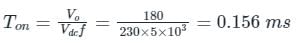
but chopping period
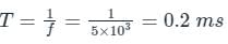
blocking period of SCR
Toff = T – Ton = 0.2 – 0.156 = 0.04347 msec = 43.47 μsec
f = 5 kHz, Vdc = 230 V, Vo = 180
but chopping period
blocking period of SCR
Toff = T – Ton = 0.2 – 0.156 = 0.04347 msec = 43.47 μsec
Assertion (A): For high power applications, inverters are used instead of transistors.
Reason (R): For high power applications, inverter is operated in active region.- a)Both A and R are true and R is the correct explanation of A.
- b)Both A and R are true but R is not the correct explanation of A.
- c)A is true but R is false.
- d)A is false but R is true.
Correct answer is option 'C'. Can you explain this answer?
Assertion (A): For high power applications, inverters are used instead of transistors.
Reason (R): For high power applications, inverter is operated in active region.
Reason (R): For high power applications, inverter is operated in active region.
a)
Both A and R are true and R is the correct explanation of A.
b)
Both A and R are true but R is not the correct explanation of A.
c)
A is true but R is false.
d)
A is false but R is true.
|
|
Nayanika Singh answered |
In low-power electronic circuits oscillators are used for converting dc power into ac power. These oscillator use transistors for converting dc voltage into sinusoidal ac voltage. Since transistor is used in active region, therefore there is substantial loss of power which decreases efficiency. In high power applications inverters are used instead of transistors and the inverters operate in saturation region or cut-off region. Thus, assertion is true but reason is false.
Assertion (A): The principal of step-up chopper can be employed for the regenerative braking of dc motors.
Reason (R) : The step-up chopper can be employed in regenerative braking only for increasing motor speeds- a)Both A and R are true and R is the correct explanation of A.
- b)Both A and R are true but R is not the correct explanation of A
- c)A is true but R is false
- d)A is false but R is true
Correct answer is option 'C'. Can you explain this answer?
Assertion (A): The principal of step-up chopper can be employed for the regenerative braking of dc motors.
Reason (R) : The step-up chopper can be employed in regenerative braking only for increasing motor speeds
Reason (R) : The step-up chopper can be employed in regenerative braking only for increasing motor speeds
a)
Both A and R are true and R is the correct explanation of A.
b)
Both A and R are true but R is not the correct explanation of A
c)
A is true but R is false
d)
A is false but R is true
|
|
Abhishek Chauhan answered |
The step-up chopper can be employed in regenerative braking both for increasing and decreasing motor speed provided duty cycle a is so adjusted that Vs/( 1 - a) exceeds the fixed source voiiage V0. Hence, reason is a false statement.
In current source inverters (CSIs), the output voltage’s- a)amplitude depends upon the load impedance
- b)waveform depends upon the load impedance
- c)amplitude as well as the nature of the waveform depends on the load
- d)both amplitude and waveform are independent of the load impedance
Correct answer is option 'C'. Can you explain this answer?
In current source inverters (CSIs), the output voltage’s
a)
amplitude depends upon the load impedance
b)
waveform depends upon the load impedance
c)
amplitude as well as the nature of the waveform depends on the load
d)
both amplitude and waveform are independent of the load impedance
|
|
Raghav Majumdar answered |
Is controlled by adjusting the modulation index of the switching signals. The modulation index represents the ratio of the amplitude of the modulating signal to the amplitude of the carrier signal. By varying the modulation index, the output voltage of the inverter can be adjusted.
CSIs use a high-frequency carrier signal to switch the power devices (such as transistors or thyristors) in the inverter. The carrier signal is usually a sinusoidal waveform with a fixed frequency. By modulating this carrier signal with a low-frequency sinusoidal waveform, the output voltage of the inverter can be controlled.
When the modulation index is increased, the amplitude of the modulating signal is increased relative to the carrier signal. This leads to a higher peak value of the output voltage waveform. Conversely, when the modulation index is decreased, the output voltage waveform has a lower peak value.
The modulation index also affects the harmonic content of the output voltage waveform. Higher modulation indices result in more harmonics, while lower modulation indices result in fewer harmonics. This is because the modulation process introduces additional frequency components to the output waveform.
Overall, the modulation index in CSIs plays a crucial role in controlling the output voltage magnitude and harmonic content. It allows for precise control of the output voltage, making CSIs widely used in applications such as motor drives, renewable energy systems, and power grid interfaces.
A d.c. source is switched in steps to synthesize the three-phase output. The basic three-phase bridge inverter can be controlled. The angle through which each switch conducts, and any instant the number of switches conducting simultaneously are, respectively- a)120° and 02
- b)120° and 03
- c)180° and 02
- d)180° and 04
Correct answer is option 'A'. Can you explain this answer?
A d.c. source is switched in steps to synthesize the three-phase output. The basic three-phase bridge inverter can be controlled. The angle through which each switch conducts, and any instant the number of switches conducting simultaneously are, respectively
a)
120° and 02
b)
120° and 03
c)
180° and 02
d)
180° and 04
|
|
Vibhor Goyal answered |
In a three-phase bridge inverter,
For 120° mode conduction, no of switches conducting simultaneously = 2
For 180° mode conduction, no of switches conducting simultaneously = 3
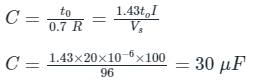
What value of capacitor (in μF) is required to forces commutate a thyristor with a turn off time of 20 μs with a 96 V battery and a full load current of 100 A.
Correct answer is between '28,32'. Can you explain this answer?
What value of capacitor (in μF) is required to forces commutate a thyristor with a turn off time of 20 μs with a 96 V battery and a full load current of 100 A.

|
Pioneer Academy answered |
The size of capacitor enquired for commutation is
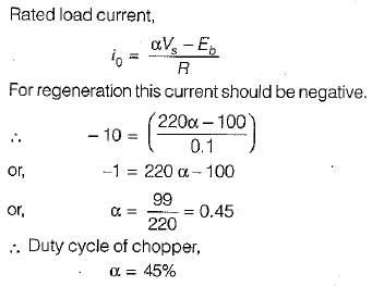
IA class C chopper is operated from a 220 V battery. The load Is a dc motor with R = 0.1Ω, L= 10 mH and Eb= 100 V. The duty cycle of the chopper to achieve regenerative braking at the rated current of 10 Ampere would be equal to- a)25%
- b)45%
- c)66%
- d)72%
Correct answer is option 'B'. Can you explain this answer?
IA class C chopper is operated from a 220 V battery. The load Is a dc motor with R = 0.1Ω, L= 10 mH and Eb= 100 V. The duty cycle of the chopper to achieve regenerative braking at the rated current of 10 Ampere would be equal to
a)
25%
b)
45%
c)
66%
d)
72%
|
|
Bhavana Reddy answered |
Inverters converts- a)dc power to dc power
- b)dc power to ac power
- c)ac power to ac power
- d)ac power to dc power
Correct answer is option 'B'. Can you explain this answer?
Inverters converts
a)
dc power to dc power
b)
dc power to ac power
c)
ac power to ac power
d)
ac power to dc power
|
|
Pooja Patel answered |
Inverter is a dc to ac converter.
In dc choppers, per unit ripple is maximum when duty cycle α is- a)0.9
- b)0.7
- c)0.5
- d)0.2
Correct answer is option 'C'. Can you explain this answer?
In dc choppers, per unit ripple is maximum when duty cycle α is
a)
0.9
b)
0.7
c)
0.5
d)
0.2

|
EduRev GATE answered |
The minimum turn-ON time of the SCR is = 

For step down chopper, Vo = δ VS
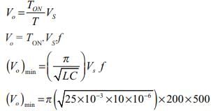
(Vo )min = 50 π V
For step down chopper, Vo = δ VS
(Vo )min = 50 π V
In a 110 V DC chopper drive using the CLC scheme, the maximum possible value of the accelerating current is 300 A. The lower limit of the current pulsation is 140 A. What is the maximum limit of current pulsation? - a)140 A
- b)440 A
- c)160 A
- d)150 A
Correct answer is option 'B'. Can you explain this answer?
In a 110 V DC chopper drive using the CLC scheme, the maximum possible value of the accelerating current is 300 A. The lower limit of the current pulsation is 140 A. What is the maximum limit of current pulsation?
a)
140 A
b)
440 A
c)
160 A
d)
150 A
|
|
Pooja Patel answered |
Current Limit Control of Chopper (CLC):
In this strategy, the chopper is turned on when the output current i0 equals a preset value I2.
The chopper is kept on till i0 increases to another preset value I1.
The chopper is turned off when i0 equals I1 and is kept off till the current i0 decays to I2.
The current i0 is thus limited to a maximum of I1 and a minimum of I2 as shown in Figure.
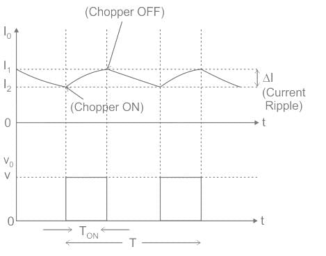
The chopping frequency and the pulse width are dependent on the load parameters.
The advantage of current limit control is that the ripple (I1 - I2), in the load current i0 can be adjusted to a small, predetermined value for a wide range of loads.
Application:
Given,
The maximum possible value of the accelerating current (I2) = 300 A
Current pulsation or current ripple (ΔI) = 140 A
The waveform can be drawn as,
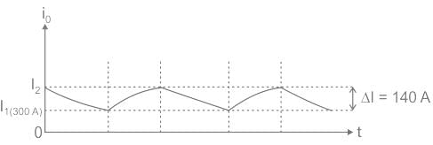
From the waveform,
The maximum limit of current pulsation (I2) = I1 + ΔI = 300 + 140 = 440 A
In this strategy, the chopper is turned on when the output current i0 equals a preset value I2.
The chopper is kept on till i0 increases to another preset value I1.
The chopper is turned off when i0 equals I1 and is kept off till the current i0 decays to I2.
The current i0 is thus limited to a maximum of I1 and a minimum of I2 as shown in Figure.
The chopping frequency and the pulse width are dependent on the load parameters.
The advantage of current limit control is that the ripple (I1 - I2), in the load current i0 can be adjusted to a small, predetermined value for a wide range of loads.
Application:
Given,
The maximum possible value of the accelerating current (I2) = 300 A
Current pulsation or current ripple (ΔI) = 140 A
The waveform can be drawn as,
From the waveform,
The maximum limit of current pulsation (I2) = I1 + ΔI = 300 + 140 = 440 A
In current source inverters- a)L filter is used after the CSI (load side)
- b)L filter is used before the CSI (input side)
- c)C filter is used after the CSI (load side)
- d)C filter is used before the CSI (input side)
Correct answer is option 'B'. Can you explain this answer?
In current source inverters
a)
L filter is used after the CSI (load side)
b)
L filter is used before the CSI (input side)
c)
C filter is used after the CSI (load side)
d)
C filter is used before the CSI (input side)
|
|
Poulomi Chopra answered |
In current source inverters, an L filter is used before the CSI (input side).
Introduction
Current Source Inverters (CSIs) are power electronic devices used to convert DC power into AC power. They are commonly used in applications such as renewable energy systems, motor drives, and uninterruptible power supplies. To improve the performance and efficiency of CSIs, filters are often employed to reduce harmonics and provide a smooth output waveform.
Purpose of Filters
Filters are used in CSIs to eliminate or reduce the harmonics generated by the switching action of the power electronic devices. Harmonics are unwanted frequencies that can distort the voltage and current waveforms, causing problems such as overheating, increased losses, and interference with other sensitive equipment. Filters help in achieving a cleaner and more sinusoidal output waveform.
Location of L Filter
In current source inverters, an L filter is used before the CSI on the input side. This means that the L filter is connected between the DC source and the CSI. The purpose of the L filter is to smooth out the current waveform supplied to the CSI, reducing the harmonics and providing a more sinusoidal current input.
Working of L Filter
The L filter consists of an inductor (L) and a capacitor (C). The inductor acts as a current source, while the capacitor acts as a voltage source. When the current flows through the inductor, it smooths out the current waveform by storing energy during the periods of high current and releasing it during the periods of low current. This helps in reducing the harmonics and providing a more sinusoidal current input to the CSI.
Advantages of Using L Filter
1. Reduced Harmonics: The L filter helps in reducing the harmonics generated by the CSI, resulting in a cleaner and more sinusoidal current waveform.
2. Improved Power Quality: By reducing the harmonics, the L filter improves the power quality of the system, preventing issues such as voltage distortion and interference with other equipment.
3. Increased Efficiency: The smoother current waveform provided by the L filter results in reduced losses and improved efficiency of the CSI.
Conclusion
In current source inverters, an L filter is used before the CSI on the input side. This filter helps in reducing the harmonics and providing a more sinusoidal current input to the CSI, resulting in improved performance and efficiency of the system.
A step-up chopper is used to deliver a load voltage of 500 V from a 220 V d.c. source. If the blocking period of the thyristor is 80 μs, the required pulse width is -- a)50.8 μs
- b)101.8 μs
- c)92.4 μs
- d)152.4 μs
Correct answer is option 'B'. Can you explain this answer?
A step-up chopper is used to deliver a load voltage of 500 V from a 220 V d.c. source. If the blocking period of the thyristor is 80 μs, the required pulse width is -
a)
50.8 μs
b)
101.8 μs
c)
92.4 μs
d)
152.4 μs
|
|
Anoushka Kumar answered |
Ms, find the duty cycle of the chopper.
The duty cycle of a chopper is defined as the ratio of the ON time of the thyristor to the total time period of one complete cycle. It is given by the formula:
Duty Cycle = (ON time of thyristor) / (Total time period)
In this case, the total time period is the sum of the ON time and the blocking time (t), which is given as 80 ms.
Total time period = ON time + blocking time = ON time + 80 ms
To find the ON time of the thyristor, we need to use the relationship between the load voltage and the input voltage in a step-up chopper, which is given by the formula:
Load voltage / Input voltage = (ON time) / (ON time + blocking time)
In this case, the load voltage is 500 V and the input voltage is 220 V.
500 V / 220 V = (ON time) / (ON time + 80 ms)
Now, we can solve for the ON time:
ON time = (500 V / 220 V) * (ON time + 80 ms)
Simplifying this equation, we get:
ON time = (500 / 220) * (ON time + 80 ms)
ON time = (500 / 220) * ON time + (500 / 220) * 80 ms
ON time - (500 / 220) * ON time = (500 / 220) * 80 ms
ON time * (1 - 500 / 220) = (500 / 220) * 80 ms
ON time * (220 - 500) / 220 = (500 / 220) * 80 ms
ON time * (-280) / 220 = (500 / 220) * 80 ms
ON time = ((500 / 220) * 80 ms) * (220 / -280)
ON time ≈ -0.1273 * 80 ms
ON time ≈ -10.18 ms
Since the ON time cannot be negative, we take the absolute value:
ON time ≈ 10.18 ms
Now, we can calculate the duty cycle:
Duty Cycle = ON time / (ON time + blocking time)
Duty Cycle = 10.18 ms / (10.18 ms + 80 ms)
Duty Cycle ≈ 10.18 ms / 90.18 ms
Duty Cycle ≈ 0.113 or 11.3%
Therefore, the duty cycle of the chopper is approximately 11.3%.
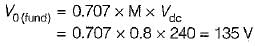
A full-bridge bipolar PWM inverter is fed from a 240 V battery and is driving an RL load. The fundamental output voltage for a modulation index of 0.8 is- a)135V
- b)215V
- c)205 V
- d)165 V
Correct answer is option 'A'. Can you explain this answer?
A full-bridge bipolar PWM inverter is fed from a 240 V battery and is driving an RL load. The fundamental output voltage for a modulation index of 0.8 is
a)
135V
b)
215V
c)
205 V
d)
165 V
|
|
Sanchita Sharma answered |
The fundamental output voltage for a modulation index of M is
In the three-phase bridge inverter, each step consists of- a)30°
- b)60°
- c)90°
- d)will depend on the value of the firing angle
Correct answer is option 'B'. Can you explain this answer?
In the three-phase bridge inverter, each step consists of
a)
30°
b)
60°
c)
90°
d)
will depend on the value of the firing angle
|
|
Subham Chaudhary answered |
° electrical angle
b)120° electrical angle
c)180° electrical angle
d)360° electrical angle
Answer: b) 120° electrical angle
b)120° electrical angle
c)180° electrical angle
d)360° electrical angle
Answer: b) 120° electrical angle
A buck converter has an input current of 2.4 A while required output current is 6 A. What will be the duty cycle of the converter? [Assume lossless system]- a)0.4
- b)1.0
- c)0.8
- d)2.0
Correct answer is option 'A'. Can you explain this answer?
A buck converter has an input current of 2.4 A while required output current is 6 A. What will be the duty cycle of the converter? [Assume lossless system]
a)
0.4
b)
1.0
c)
0.8
d)
2.0

|
Engineers Adda answered |
Concept:
In a buck converter, the output voltage is given by
Vo = δVin
and Iin = δIo
Where Vo is the output voltage
Vin is the input voltage
Iin is the input current
Io is the output current
δ is the duty cycle
Calculation:
Given that, input current (Iin) = 2.4 A
Output current (Io) = 6 A
Duty cycle, 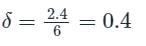
Assertion (A): The terminal voltage of a voltage source inverter remains substantially constant with variations in load.
Reason (R): Any short-circuit across the terminals of a voltage source inverter causes current to rise very fast.- a)Both A and R are true and R is the correct explanation of A
- b)Both A and R are true but R is not the correct explanation of A
- c)A is true but R is false
- d)A is false but R is true
Correct answer is option 'B'. Can you explain this answer?
Assertion (A): The terminal voltage of a voltage source inverter remains substantially constant with variations in load.
Reason (R): Any short-circuit across the terminals of a voltage source inverter causes current to rise very fast.
Reason (R): Any short-circuit across the terminals of a voltage source inverter causes current to rise very fast.
a)
Both A and R are true and R is the correct explanation of A
b)
Both A and R are true but R is not the correct explanation of A
c)
A is true but R is false
d)
A is false but R is true
|
|
Sharmila Bajaj answered |
Explanation:
The correct answer is option 'B': Both A and R are true but R is not the correct explanation of A.
Assertion (A): The terminal voltage of a voltage source inverter remains substantially constant with variations in load.
Reason (R): Any short-circuit across the terminals of a voltage source inverter causes current to rise very fast.
Explanation:
Terminal Voltage of a Voltage Source Inverter:
- A voltage source inverter (VSI) is an electronic device that converts a DC voltage source into an AC voltage source.
- The terminal voltage of a VSI refers to the voltage across the output terminals of the inverter.
- Ideally, the terminal voltage of a VSI should remain constant with variations in load.
Reason Explanation:
- The reason states that any short-circuit across the terminals of a VSI causes current to rise very fast.
- This statement is true because in a short-circuit condition, the impedance across the terminals becomes very low, resulting in a high current flow.
- However, this reason does not directly explain why the terminal voltage of a VSI remains constant with load variations.
Explanation of Assertion:
- The assertion states that the terminal voltage of a VSI remains substantially constant with variations in load.
- This assertion is true because VSIs are designed to regulate the output voltage regardless of the load variations.
- VSIs achieve this regulation by using control techniques such as pulse width modulation (PWM).
- PWM adjusts the width of the output pulses based on the load requirements, ensuring that the average output voltage remains constant.
Conclusion:
- Both the assertion and reason are true.
- However, the reason does not provide a correct explanation for the assertion.
- The terminal voltage of a VSI remains constant with variations in load due to the control techniques used, not solely because of the potential of a short-circuit.
A four-quadrant chopper is driving a separately excited dc motor load. The motor parameters are R = 0.1 Ω, L = 10 mH. The supply voltage is 200 V d.c. If the rated current of the motor is 10 A with Eb = 150 V and motor is driving the rated torque, then it is operating under- a)forward motoring mode
- b)reverse braking mode
- c)reverse motoring mode
- d)forward brakina mode
Correct answer is option 'A'. Can you explain this answer?
A four-quadrant chopper is driving a separately excited dc motor load. The motor parameters are R = 0.1 Ω, L = 10 mH. The supply voltage is 200 V d.c. If the rated current of the motor is 10 A with Eb = 150 V and motor is driving the rated torque, then it is operating under
a)
forward motoring mode
b)
reverse braking mode
c)
reverse motoring mode
d)
forward brakina mode
|
|
Hiral Kulkarni answered |
For a four-quadrant chopper, the average voltage in all the four-modes is given by
V0 = 2 Vs (α - 0.5)
The average curreni,
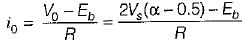
or,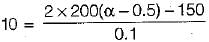
or, α = 0.877
Since α > 0.5, the motor is operating undi
forward motorina mode.
V0 = 2 Vs (α - 0.5)
The average curreni,
or,
or, α = 0.877
Since α > 0.5, the motor is operating undi
forward motorina mode.
In a single-pulse modulation of PWM inverters if pulse width is 120° then- a)5th harmonic will be eliminated
- b)3rd harmonic will be eliminated
- c)7th harmonic will be eliminated
- d)none of the above
Correct answer is option 'B'. Can you explain this answer?
In a single-pulse modulation of PWM inverters if pulse width is 120° then
a)
5th harmonic will be eliminated
b)
3rd harmonic will be eliminated
c)
7th harmonic will be eliminated
d)
none of the above
|
|
Manoj Chaudhary answered |
The rms value of amplitude of harmonic voltage of a single, pulse modulated wave is given by
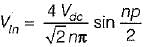
(where, p = width of pulse an Vdc = supply dc voltage)
If the 3rd harmonic Is to be eliminated, then
EL3 = 0
i.e.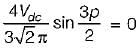
or,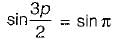
or,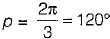
= Required pulse width
(where, p = width of pulse an Vdc = supply dc voltage)
If the 3rd harmonic Is to be eliminated, then
EL3 = 0
i.e.
or,
or,
= Required pulse width
In a VSI (Voltage source inverter)- a)the internal impedance of the DC source is negligible
- b)the internal impedance of the DC source is very very high
- c)the internal impedance of the AC source is negligible
- d)the IGBTs are fired at 0 degrees.
Correct answer is option 'A'. Can you explain this answer?
In a VSI (Voltage source inverter)
a)
the internal impedance of the DC source is negligible
b)
the internal impedance of the DC source is very very high
c)
the internal impedance of the AC source is negligible
d)
the IGBTs are fired at 0 degrees.
|
|
Pooja Patel answered |
A VSI is the one in which the internal impedance of the source is negligible. It has a stiff DC source at its input.
Single phase half bridge inverters requires- a)two wire ac supply
- b)two wire dc supply
- c)three wire ac supply
- d)three wire dc supply
Correct answer is option 'D'. Can you explain this answer?
Single phase half bridge inverters requires
a)
two wire ac supply
b)
two wire dc supply
c)
three wire ac supply
d)
three wire dc supply
|
|
Rahul Banerjee answered |
Single Phase Half Bridge Inverters and Their Requirements
Introduction:
Single-phase half bridge inverters are a type of power electronic device used to convert DC (direct current) power into AC (alternating current) power. They are commonly used in applications such as motor drives, renewable energy systems, and uninterruptible power supplies (UPS). To operate efficiently and effectively, these inverters require specific types of power supplies.
Explanation:
1. Two-Wire AC Supply:
- A two-wire AC supply refers to a single-phase AC source with two conductors: one live (active) wire and one neutral wire.
- While it is possible to operate a single-phase half bridge inverter with a two-wire AC supply, it is not the most common or efficient configuration.
- In this setup, the inverter requires an additional circuitry to create a virtual neutral point, which can increase complexity and cost.
2. Two-Wire DC Supply:
- A two-wire DC supply refers to a DC power source with two terminals: positive and negative.
- Single-phase half bridge inverters cannot be directly connected to a two-wire DC supply since they require a bipolar voltage source.
- Bipolar voltage sources provide both positive and negative voltage levels required for the inverter operation.
3. Three-Wire AC Supply:
- A three-wire AC supply refers to a single-phase AC source with three conductors: one live (active) wire, one neutral wire, and one ground wire.
- This is the most common and efficient configuration for single-phase half bridge inverters.
- The inverter can be directly connected to the three-wire AC supply without the need for additional circuitry.
- The live wire provides the necessary AC voltage, the neutral wire completes the circuit, and the ground wire ensures safety.
4. Three-Wire DC Supply:
- A three-wire DC supply is not a common configuration in power electronics.
- While it is possible to create a three-wire DC supply using additional circuitry, it is not a standard requirement for single-phase half bridge inverters.
- Typically, the DC supply used for these inverters is a two-wire bipolar voltage source.
Conclusion:
The correct answer is option D, which states that single-phase half bridge inverters require a three-wire DC supply. This is because a three-wire DC supply is not a standard requirement for these inverters. Instead, they are commonly connected to a three-wire AC supply, which provides the necessary voltage and circuit completion.
Force-commutated CSIs need- a)capacitors for their commutation
- b)inductors for their commutation
- c)diodes for their commutation
- d)none of the mentioned
Correct answer is option 'A'. Can you explain this answer?
Force-commutated CSIs need
a)
capacitors for their commutation
b)
inductors for their commutation
c)
diodes for their commutation
d)
none of the mentioned
|
|
Pooja Patel answered |
All the CSIs need capacitors for their commutation if force commutation is required. Force commutation is essential for lagging power factors.
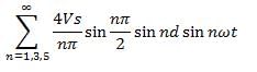
In the single-pulse width modulation method, the Fourier coefficient bn is given by- a)(Vs/π) [sin(nπ/2) sin(nd)].
- b)0
- c)(4Vs/nπ) [sin(nπ/2) sin(nd)].
- d)(2Vs/nπ) [sin(nπ/2) sin(nd)].
Correct answer is option 'C'. Can you explain this answer?
In the single-pulse width modulation method, the Fourier coefficient bn is given by
a)
(Vs/π) [sin(nπ/2) sin(nd)].
b)
0
c)
(4Vs/nπ) [sin(nπ/2) sin(nd)].
d)
(2Vs/nπ) [sin(nπ/2) sin(nd)].
|
|
Sanjana Chopra answered |
In the single-pulse width modulation method, the Fourier coefficient bn is given by:
bn = (2Vs/T) * ∫[t_on, t_off] sin(nωt)dt
where bn is the nth Fourier coefficient, Vs is the amplitude of the sine wave that is being modulated, T is the period of the modulation signal, t_on is the starting time of the pulse, t_off is the ending time of the pulse, ω is the angular frequency (2πf) of the sine wave, and n is the order of the Fourier coefficient.
Consider the boost converter of the input voltage to this converter is 6 V. The average output voltage is Vo = 18 V and the average load current Io = 0.4 A. If the switching frequency is 20 kHz for L = 250 μH, then the ripple current of inductor is _______A.- a)1 A
- b)2.5 A
- c)3 A
- d)0.8 A
Correct answer is option 'D'. Can you explain this answer?
Consider the boost converter of the input voltage to this converter is 6 V. The average output voltage is Vo = 18 V and the average load current Io = 0.4 A. If the switching frequency is 20 kHz for L = 250 μH, then the ripple current of inductor is _______A.
a)
1 A
b)
2.5 A
c)
3 A
d)
0.8 A
|
|
Sparsh Saini answered |
To find the inductor value (L) for the boost converter, we can use the following equation:
L = (Vo * (Vin - Vo)) / (Vin * F * Io)
where:
Vo = average output voltage = 18 V
Vin = input voltage = 6 V
F = switching frequency = 20 kHz
Io = average load current = 0.4 A
Plugging in the given values:
L = (18 * (6 - 18)) / (6 * 20,000 * 0.4)
L = (-180) / (4,800)
L = -0.0375 H
However, it is not physically possible to have a negative inductance value. Therefore, there may be an error in the given values or calculation. Please double-check the values and provide the correct information for a valid calculation.
A step-up chopper is fed with 200 V. The conduction time of the thyristor is 200 µs and the required output is 600 V. If the frequency of operation is kept constant and the pulse width is halved, what will be the new output voltage?- a)600 volts
- b)300 volts
- c)400 volts
- d)200 volts
Correct answer is option 'B'. Can you explain this answer?
A step-up chopper is fed with 200 V. The conduction time of the thyristor is 200 µs and the required output is 600 V. If the frequency of operation is kept constant and the pulse width is halved, what will be the new output voltage?
a)
600 volts
b)
300 volts
c)
400 volts
d)
200 volts
|
|
Vibhor Goyal answered |
Formula:
Where, Vo is the output voltage
Vin is the input voltage
TON is the pulse width
Application:
Given,
Vin = 200 volts
TON = 200 µs
V0 = 600 V
From equation (1),
or, 3T - 600 = T
Hence, T = 300 µs
If the Pulse width is half then, the new value of pulse width (TON') will be,
Hence,
Hence, the new value of output voltage (V0') will be,

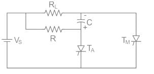
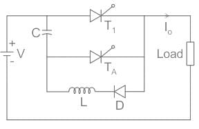
Consider the circuit shown below:
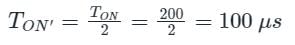
The effective on period of the chopper if V =230 V,Io = 60 A,C = 55 μF,Ton = 800 μs is:- a)1.22 ms
- b)1.07 ms
- c)1.85 ms
- d)1.47 ms
Correct answer is option 'A'. Can you explain this answer?
Consider the circuit shown below:
The effective on period of the chopper if V =230 V,Io = 60 A,C = 55 μF,Ton = 800 μs is:
The effective on period of the chopper if V =230 V,Io = 60 A,C = 55 μF,Ton = 800 μs is:
a)
1.22 ms
b)
1.07 ms
c)
1.85 ms
d)
1.47 ms

|
Naroj Boda answered |
Concept:
Mode 1: T1 will remain ON and conduct to load and diode TA will remain OFF
Mode 2: TA will be turned ON; the capacitor current will now flow in reverse direction & T1 stops conducting.
Therefore, the effective time period of the chopper is
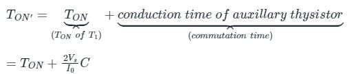
Commutation time: It is the time taken to disconnect the load from the supply after the main thyristor is turned OFF.
Calculation:
Effective on period
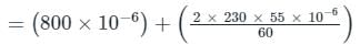
= (0.8 + 0.42) × 10-3
TON’ = 1.22 ms
Mode 1: T1 will remain ON and conduct to load and diode TA will remain OFF
Mode 2: TA will be turned ON; the capacitor current will now flow in reverse direction & T1 stops conducting.
Therefore, the effective time period of the chopper is
Commutation time: It is the time taken to disconnect the load from the supply after the main thyristor is turned OFF.
Calculation:
Effective on period
= (0.8 + 0.42) × 10-3
TON’ = 1.22 ms
A current source inverter can be- a)load commutated
- b)force commutated
- c)either load or force commutated
- d)neither load nor force commutated
Correct answer is option 'C'. Can you explain this answer?
A current source inverter can be
a)
load commutated
b)
force commutated
c)
either load or force commutated
d)
neither load nor force commutated
|
|
Gaurav Chauhan answered |
A CSl can be either load commutated or force commutated.
VSIs using GTOs are turned off by- a)load commutation
- b)line commutation
- c)applying a negative gate pulse
- d)removing the base signal
Correct answer is option 'C'. Can you explain this answer?
VSIs using GTOs are turned off by
a)
load commutation
b)
line commutation
c)
applying a negative gate pulse
d)
removing the base signal
|
|
Pooja Patel answered |
GTOs are gate turn off SCRs in which turn-off is achieved by applying a negative gate pulse.
A CSI converters- a)the input dc current to an an current at output
- b)the input ac current to dc current at output
- c)the input dc current to amplified dc current at the output
- d)the input ac current to amplified ac current at the output
Correct answer is option 'A'. Can you explain this answer?
A CSI converters
a)
the input dc current to an an current at output
b)
the input ac current to dc current at output
c)
the input dc current to amplified dc current at the output
d)
the input ac current to amplified ac current at the output
|
|
Pooja Patel answered |
CSI converts the input dc current to an ac current at its output terminals.
A three-phase bridge inverter requires minimum of _______ switching devices.- a)3
- b)4
- c)6
- d)8
Correct answer is option 'C'. Can you explain this answer?
A three-phase bridge inverter requires minimum of _______ switching devices.
a)
3
b)
4
c)
6
d)
8
|
|
Anirban Gupta answered |
Introduction:
A three-phase bridge inverter is a type of power electronic device used to convert DC power into AC power. It is widely used in various applications such as motor drives, renewable energy systems, and grid-tied inverters. The bridge inverter consists of switching devices that are used to control the flow of current in the inverter circuit.
Explanation:
To understand why a minimum of six switching devices are required for a three-phase bridge inverter, let's first take a look at the basic structure of the inverter.
Basic Structure:
A three-phase bridge inverter consists of three legs, with each leg consisting of two switching devices. Each leg is connected to one phase of the three-phase AC output. The switching devices in each leg are typically semiconductor devices such as power transistors or insulated gate bipolar transistors (IGBTs). The switching devices are controlled by a pulse width modulation (PWM) technique to generate the desired AC output waveform.
Working Principle:
During the positive half-cycle of the AC output waveform, the switching devices in one leg are turned on, while the switching devices in the other two legs are turned off. This allows the current to flow through the load in the intended direction. During the negative half-cycle, the switching devices in the other two legs are turned on, and the switching devices in the first leg are turned off. This reverses the direction of current flow through the load. By controlling the switching devices in each leg, the desired AC output waveform can be generated.
Switching Devices:
In a three-phase bridge inverter, each leg requires two switching devices to control the flow of current. Since there are three legs in total, we need a minimum of six switching devices. These switching devices can be arranged in different configurations, such as a half-bridge or a full-bridge configuration, depending on the specific requirements of the application.
Conclusion:
In conclusion, a three-phase bridge inverter requires a minimum of six switching devices. These switching devices are used to control the flow of current in each leg of the inverter circuit. By properly controlling the switching devices, the desired AC output waveform can be generated.
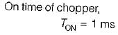
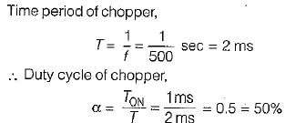
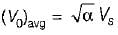
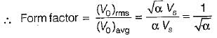
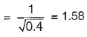
A single-quadrant type A chopper is operating with the following specifications:
Ideal battery of 220 V;
on-time ton - 1 ms;
off-time foff = 1.5 ms
The ripple and form factors will be respectively given by- a)0.98 and 1.20
- b)1.58 and 1.22
- c)1.22 and 1.58
- d)1.58 and 1.20
Correct answer is option 'C'. Can you explain this answer?
A single-quadrant type A chopper is operating with the following specifications:
Ideal battery of 220 V;
on-time ton - 1 ms;
off-time foff = 1.5 ms
The ripple and form factors will be respectively given by
Ideal battery of 220 V;
on-time ton - 1 ms;
off-time foff = 1.5 ms
The ripple and form factors will be respectively given by
a)
0.98 and 1.20
b)
1.58 and 1.22
c)
1.22 and 1.58
d)
1.58 and 1.20
|
|
Juhi Joshi answered |
For a type-A chopper, average output voltage
A single-phase full bridge inverter can operate in load-commutation mode in case load consists of- a)RLC critically damped
- b)RLC underdamped
- c)RLC overdamped
- d)RC
Correct answer is option 'B'. Can you explain this answer?
A single-phase full bridge inverter can operate in load-commutation mode in case load consists of
a)
RLC critically damped
b)
RLC underdamped
c)
RLC overdamped
d)
RC
|
|
Bijoy Mehta answered |
In a 1-φ full bridge inverter if RLC load is underdamped, then the two thyristors (namely T1 and T2) shown in figure will get commutated naturally and therefore no commutation circuitry will be needed. Thus, load commutation will be possible.
VSIs using IGBTs are turned off by- a)load commutation
- b)line commutation
- c)applying a negative gate pulse
- d)removing the base signal
Correct answer is option 'D'. Can you explain this answer?
VSIs using IGBTs are turned off by
a)
load commutation
b)
line commutation
c)
applying a negative gate pulse
d)
removing the base signal
|
|
Pooja Patel answered |
IGBT is a transistor family device. It can be turned off simply by removing the gate signal. All the transistor devices operated in the same way in inverters.
__________ based inverters do not require self-commutation.- a)IGBT
- b)GTO
- c)PMOSFET
- d)SCR
Correct answer is option 'D'. Can you explain this answer?
__________ based inverters do not require self-commutation.
a)
IGBT
b)
GTO
c)
PMOSFET
d)
SCR
|
|
Pooja Patel answered |
All the devices can be turned off by their gate/base singles expect SCR. SCRs require external commutation circuits.
In the single-pulse width modulation method, when the pulse width of 2d is equal to its maximum value of π radians, then the fundamental component of output voltage is given by- a)Vs
- b)4Vs/π
- c)0
- d)2Vs/π
Correct answer is option 'B'. Can you explain this answer?
In the single-pulse width modulation method, when the pulse width of 2d is equal to its maximum value of π radians, then the fundamental component of output voltage is given by
a)
Vs
b)
4Vs/π
c)
0
d)
2Vs/π
|
|
Pooja Patel answered |
The Fourier representation of the output voltage is given by
Put 2d = π & n = 1.
Put 2d = π & n = 1.
In a 3-phase inverter with 180° conduction mode the number of switches that is on at any instant of time is- a)1
- b)2
- c)3
- d)4
Correct answer is option 'C'. Can you explain this answer?
In a 3-phase inverter with 180° conduction mode the number of switches that is on at any instant of time is
a)
1
b)
2
c)
3
d)
4

|
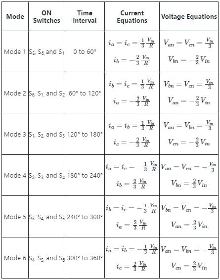
Bayshore Academy answered |
180-degree conduction with star connected resistive load:
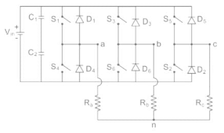
The configuration of the three-phase inverter with star connected resistive load as shown in the figure. The following convention is followed.
- A current leaving a node point a, b or c and entering the neutral point n is assumed to be positive.
- All the three resistances are equal, Ra = Rb = Rc = R
In this mode of operation, each switch conducts for 180°. Hence at any instant of time three switches remain on. There are six possible modes of operation in a cycle and each mode is of 60° duration and the explanation of each mode is as follows:
In voltage source inverters (VSIs), the amplitude of the output voltage is- a)independent of the load
- b)dependent on the load
- c)dependent only on L loads
- d)none of the mentioned
Correct answer is option 'A'. Can you explain this answer?
In voltage source inverters (VSIs), the amplitude of the output voltage is
a)
independent of the load
b)
dependent on the load
c)
dependent only on L loads
d)
none of the mentioned
|
|
Bijoy Mehta answered |
The Amplitude of the Output Voltage in Voltage Source Inverters (VSIs)
Introduction:
Voltage source inverters (VSIs) are electronic devices used in power electronic systems to convert DC (direct current) power into AC (alternating current) power. They are commonly used in applications such as motor drives, renewable energy systems, and power grid interfaces. One of the key characteristics of VSIs is the amplitude of the output voltage.
Explanation:
The amplitude of the output voltage in voltage source inverters (VSIs) is independent of the load. This means that it remains constant regardless of the type or magnitude of the load connected to the inverter. This is a desirable feature in many applications where a stable AC voltage is required.
Reasons:
There are a few reasons why the amplitude of the output voltage in VSIs is independent of the load:
- PWM Technique: VSIs utilize Pulse Width Modulation (PWM) techniques to control the output voltage. PWM involves switching the DC input voltage on and off at a high frequency to create an AC waveform. The amplitude of the output voltage is determined by the duty cycle of the PWM signal, which remains constant regardless of the load.
- Feedback Control: VSIs often incorporate feedback control mechanisms to regulate the output voltage. These control systems continuously monitor the output voltage and adjust the PWM signal to maintain a constant amplitude. This feedback control compensates for any variations in the load and ensures a stable output voltage.
- Constant Voltage Source: The name "voltage source inverter" itself implies that the inverter is designed to act as a constant voltage source. This means that it strives to maintain a fixed output voltage regardless of the load conditions. The internal circuitry of the inverter is designed to achieve this constant voltage output.
Advantages:
The independence of the output voltage amplitude from the load in VSIs offers several advantages:
- Stable Operation: Regardless of the connected load, the VSI provides a stable and consistent output voltage, which is essential for many applications.
- Compatibility: The load independence allows VSIs to be used with a wide range of electrical loads without the need for additional adjustments or modifications.
- Flexibility: The load independence simplifies the design and operation of power electronic systems that incorporate VSIs, as the focus can be placed on other aspects such as efficiency and control rather than worrying about load variations.
Conclusion:
In summary, the amplitude of the output voltage in voltage source inverters (VSIs) is independent of the load. This characteristic is achieved through the use of PWM techniques, feedback control, and the inherent design of VSIs as constant voltage sources. Understanding this behavior is crucial for the successful implementation of VSIs in various power electronic applications.
A single-phase half-bridge inverter has a resistive load of R = 3 Ω and the dc input voltage Vdc = 24 volts. The harmonic factor of the lowest order harmonic would be equal to - a)33.33%
- b)25.0%
- c)66.67%
- d)50.0%
Correct answer is option 'A'. Can you explain this answer?
A single-phase half-bridge inverter has a resistive load of R = 3 Ω and the dc input voltage Vdc = 24 volts. The harmonic factor of the lowest order harmonic would be equal to
a)
33.33%
b)
25.0%
c)
66.67%
d)
50.0%
|
|
Ashutosh Majumdar answered |
The lowest harmonic is third harmonic
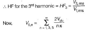
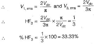
Chapter doubts & questions for Principles of Thyristor Choppers and Inverters - Electrical Engineering Optional Notes for UPSC 2025 is part of UPSC CSE exam preparation. The chapters have been prepared according to the UPSC CSE exam syllabus. The Chapter doubts & questions, notes, tests & MCQs are made for UPSC CSE 2025 Exam. Find important definitions, questions, notes, meanings, examples, exercises, MCQs and online tests here.
Chapter doubts & questions of Principles of Thyristor Choppers and Inverters - Electrical Engineering Optional Notes for UPSC in English & Hindi are available as part of UPSC CSE exam.
Download more important topics, notes, lectures and mock test series for UPSC CSE Exam by signing up for free.
Electrical Engineering Optional Notes for UPSC
550 videos|588 docs|343 tests
|
|
© EduRev
|
Education Revolution
|


|


Signup on EduRev and stay on top of your study goals
10M+ students crushing their study goals daily